Technical
Assembly
Technical
Assembly
What is PCB Surface Treatment?
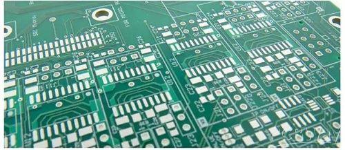
PCB surface treatment refers to the metal interconnections between the exposed copper and components in the solderable areas of a printed circuit board (PCB). A PCB has a copper substrate, which can easily oxidize without a protective coating, hence the need for surface finish.
PCB surface treatment is one of the most critical steps in PCB manufacturing and assembly, serving two primary functions: one is to protect the exposed copper circuits, and the other is to provide a solderable surface for components to attach to the PCB. As shown in the diagram below, the surface treatment is located on the outer layer of the PCB, on top of the copper layer, acting as a “coating” for the copper.
Types of PCB Surface Treatment
- Hot Air Solder Leveling (HASL)
- Immersion Tin (ImSn)
- Electroless Nickel Immersion Gold (ENIG)
- Organic Solderability Preservative (OSP)
- Immersion Silver (ImAg)
- Electroless Nickel Electroless Palladium Immersion Gold (ENEPIG)
- Hard Gold (Electrolytic Hard Gold)
PCB Surface Treatment Processes
Hot Air Solder Leveling (HASL)
Hot Air Solder Leveling (HASL) is one of the most commonly used surface treatment methods in the industry. HASL is divided into two types: leaded and lead-free solder. It is also one of the cheapest types of PCB surface treatment available.
To form a HASL surface finish, the circuit board is immersed in molten solder (tin/lead), which covers all exposed copper surfaces of the board. After leaving the molten solder, high-pressure hot air is blown over the surface using an air knife, leveling the solder deposits and removing excess solder from the PCB surface.
Several critical parameters must be controlled during this process: soldering temperature, air knife temperature, air knife pressure, immersion time, and lift speed.
The key points for PCB hot air leveling are:
- The PCB should be immersed in molten solder.
- The air knife blows away the liquid solder before it solidifies.
- The air knife minimizes solder meniscus on the copper surface and prevents solder bridging.
Due to surface roughness issues, HASL has limitations for SMT (Surface Mount Technology) applications and cannot be used for tactile switches.
If the PCB is subjected to high temperatures, copper may dissolve, especially in thick or thin boards, which makes soldering challenging.
Advantages and Disadvantages of Hot Air Solder Leveling (HASL)
Advantages:
- Abundant supply
- Reworkable
- Excellent shelf life
- Outstanding solderability
- Cost-effective
- Allows for larger processing windows
- Longer storage time
- The pads are completely covered with solder before soldering
- Suitable for lead-free soldering
- A mature surface treatment option
- Allows for visual inspection and electrical measurement
Disadvantages:
- Uneven surface
- Not suitable for fine pitch
- Leaded (HASL)
- Thermal shock
- Solder bridging
- Reduced PTH (Plated Through Hole)
- Thickness/morphology differences between large and small pads
- Not suitable for SMD and BGA with pitches smaller than 20 mils
- Not suitable for HDI products
- Not suitable for wire bonding
Immersion Tin (ImSn)
Immersion Tin (ImSn) is a metal finish deposited through a chemical displacement reaction, directly applied to the substrate metal of the circuit board (i.e., copper).
ImSn protects the underlying copper from oxidation during its intended shelf life. Since all solder is tin-based, the tin layer can match any type of solder.
Adding organic additives to the tin immersion solution creates a granular structure in the tin layer, overcoming issues related to tin whiskers and tin migration while maintaining good thermal stability and solderability.
The immersion tin process can form a flat copper-tin intermetallic compound, providing good solderability without issues related to flatness or intermetallic compound diffusion.
Advantages and Disadvantages of Immersion Tin (ImSn)
Advantages:
- Provides excellent flatness (suitable for SMT), suitable for fine pitch/BGA/smaller components.
- A medium-cost lead-free surface treatment technology.
- Achieves suitable flatness.
- Maintains good solderability after multiple thermal excursions.
- Suitable for horizontal production lines.
- Suitable for fine geometry and lead-free assembly.
Disadvantages:
- Sensitive to processing.
- Short shelf life; tin whiskers may appear after 6 months.
- Corrosive to solder mask.
- Not recommended for use with removable masks.
- Not suitable for tactile switches.
- Electrical testing requires special setups (soft probe landing).
Electroless Nickel Immersion Gold (ENIG)
ENIG (Electroless Nickel Immersion Gold) surface treatment is traditionally considered the best option for fine pitch (flat) surfaces and lead-free applications.
ENIG is a two-step process, applying a thin layer of nickel followed by a thin layer of gold. Nickel serves as a barrier between the copper and the soldering surface, while gold protects the nickel from oxidation during storage.
The typical thickness of Ni is about 3-6 μm, and the deposited thickness of Au is about 0.05-0.1 μm.
Ni acts as a barrier layer between solder and copper.
Au prevents Ni from oxidizing during storage, thereby extending the shelf life, while the gold plating process also produces excellent surface flatness.
The ENIG treatment process is as follows: cleaning → etching → catalysis → electroless nickel plating → gold plating → cleaning of residues.
Although this coating process has a long shelf life and is beneficial for plated through holes, it is a complex and expensive process, cannot be reworked, and is known to cause losses in RF signal circuits.
Advantages and Disadvantages of Electroless Nickel Immersion Gold (ENIG)
Advantages:
- Flat surface
- Lead-free
- Suitable for PTH (Plated Through Hole)
- Long shelf life
Disadvantages:
- Expensive
- Not reworkable
- Black pad/black nickel issues
- RF signal losses
- Complex process
Organic Solderability Preservative (OSP)
OSP (Organic Solderability Preservative) or anti-corrosion agents typically involves applying a very thin protective layer of material over exposed copper using a conveyor belt process to protect the copper surface from oxidation.
This film must possess properties such as anti-oxidation, thermal shock resistance, and moisture resistance to prevent rust (oxidation or sulfide, etc.) under normal environmental conditions.
However, during subsequent high-temperature soldering, this protective film must be easily removed by the flux, allowing the clean exposed copper surface to bond immediately with molten solder, forming a strong solder joint in a very short time.
In other words, the role of OSP is to act as a barrier between copper and air.
The general process for OSP is: degreasing → micro-etching → acid washing → pure water washing → organic coating → cleaning.
OSP uses a water-based organic compound that selectively binds with copper, providing an organic metallic layer that protects copper before soldering. Compared to other common lead-free finishes, it is also very environmentally friendly, as the latter are more toxic or energy-intensive.
Advantages and Disadvantages of Organic Solderability Preservative (OSP)
Advantages:
- Flat surface
- Simple process, very smooth surface, lead-free soldering, and SMT
- Reworkable, suitable for horizontal production lines
- Cost-effective
- Environmentally friendly
Disadvantages:
- Thickness cannot be measured
- Not suitable for PTH (Plated Through Hole)
- Short shelf life
- May cause ICT (In-Circuit Testing) issues
- Exposed copper during final assembly
- Sensitive to processing
- Cannot be soldered (reworked) more than twice
- Not suitable for crimping techniques and wire bonding
- Inconvenient for visual and electrical measurement
- Requires injection of nitrogen oxides for SMT
Immersion Silver (ImAg)
Immersion Silver is a non-electrolytic chemical surface treatment applied by immersing the copper PCB in a silver ion bath. It is ideal for circuit boards with EMI shielding and is also used for dome contacts and wire bonding. The average surface thickness of silver is 5-18 microinches.
Considering modern environmental issues such as RoHS and WEEE, immersion silver is more environmentally friendly than HASL and ENIG. It is also popular because its cost is lower than that of ENIG.
Even PCBs processed through immersion silver can provide good electrical performance and maintain good solderability when exposed to high temperatures, humidity, and contaminated environments, although they may lose their luster.
Immersion silver is a displacement reaction that deposits a layer of pure silver directly onto copper.
Sometimes, immersion silver is combined with OSP coatings to prevent the silver from reacting with sulfides in the environment.
Common applications include flat requirements, which may include:
- Membrane switches
- EMI shielding
- Aluminum wire bonding
- Very fine traces
Advantages and Disadvantages of Immersion Silver (ImAg)
Advantages:
- High solderability.
- Good surface flatness.
- Low cost and lead-free (compliant with RoHS standards).
- Suitable for aluminum wire bonding.
Disadvantages:
- High storage requirements.
- Prone to contamination.
- Short assembly window after removal from packaging.
- Difficult to perform electrical testing.
Electroless Nickel Electroless Palladium Immersion Gold (ENEPIG)
The ENEPIG surface finish consists of a copper-nickel-palladium-gold layer structure, allowing direct wire bonding to the coating. The last layer of gold is very thin, similar to that in ENIG. The gold layer is a protection layer, while the palladium layer prevents oxidation of the nickel layer, increasing solderability.
The primary advantage of ENEPIG is that it is suitable for both surface mounting and wire bonding applications.
Advantages and Disadvantages of Electroless Nickel Electroless Palladium Immersion Gold (ENEPIG)
Advantages:
- Good solderability.
- Prevents oxidation of the nickel layer.
- Suitable for surface mount and wire bonding applications.
Disadvantages:
- More expensive than traditional finishes.
- More complex processing.
Hard Gold (Electrolytic Hard Gold)
Hard gold is an electrolytic gold plating process that deposits a thicker gold layer (approximately 2-6 μm) than that found in other surface finishes. The plating is performed using a nickel base, which is an expensive process.
Hard gold plating provides excellent wear resistance, making it suitable for applications with high physical and mechanical performance. It is mainly used for connectors, switch contacts, and other high-reliability applications, but it is not suitable for PCB soldering.


