
Technical
Assembly
Technical
Assembly
PCB Assembly Testing and Inspection
A PCB assembly can look complete and still have a misplaced component, an inaccessible solder joint or a function that does not respond as expected. Finding these issues before shipment requires a test plan suited to the board—not simply a list of equipment.
GreatPCB supports PCB assembly projects from prototype to production. We can discuss the inspection and testing requirements for your design alongside the assembly scope, component packages, production quantity and acceptance criteria. Confirm the selected methods, coverage and reporting requirements for your order before production.
What Does PCB Assembly Testing Check?
PCB assembly testing and inspection examine a populated circuit board after components are placed and soldered. Some methods look for visible assembly defects; others use electrical measurements or operate selected functions of the board. Each answers a different question.
| What needs checking | Examples | Methods to consider | What the result does not establish on its own |
|---|---|---|---|
| Component placement and visible solder joints | Missing components, orientation, visible bridges or solder features | Manual inspection and automated optical inspection (AOI) | The operation of the assembled circuit or joints hidden beneath a package |
| Hidden solder joints | Selected BGA or QFN connections, bridges or voids | X-ray inspection, according to the inspection plan | Firmware behavior or operation under every condition |
| Electrical features at accessible points | Selected opens, shorts or component values | In-circuit measurements using a fixture or flying probes | Features outside the available access and programmed tests |
| Board operation | Power-up, an output, an interface or another specified function | Functional test (FCT) | Performance outside the tested modes and limits, or long-term reliability |
For example, AOI might flag a visibly displaced resistor, while a functional test checks whether a defined output behaves correctly. A board can pass one check and still need another: a good-looking board may fail to communicate, and a board that communicates during one test may still have a defect outside that test’s scope.
Bare-board and assembled-board testing serve different stages. A bare PCB has no components installed. Its electrical test checks specified connections and isolation before assembly; component placement and operating functions need their own checks afterward. See our bare-board PCB testing page for fabrication inspection and electrical testing.
PCB Assembly Inspection Methods
Manual Visual Inspection
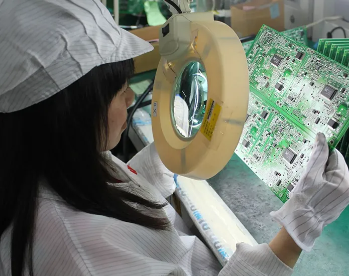
An inspector examines accessible parts of the assembly for issues such as damaged components, obvious placement errors, solder bridges or contamination. Magnification can help with small features, and a defined acceptance standard gives the inspector a consistent basis for deciding what to review.
Manual inspection is also useful when an automated system flags a potential defect. The operator can examine the flagged area, compare it with the drawing or acceptance criteria and decide whether further investigation is needed.
Its effectiveness depends on access, visibility, the inspection criteria and the features being examined. A joint underneath a package may not be visible even under magnification.
Automated Optical Inspection (AOI)
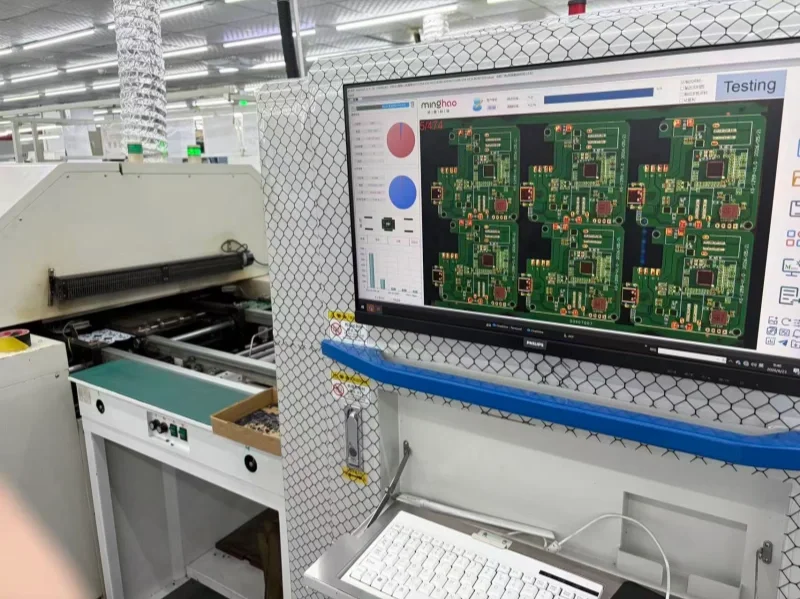
AOI uses cameras and programmed inspection criteria to examine visible features of the assembly. Depending on the equipment and program, it can flag missing or misaligned components, orientation issues and selected solder-joint defects.
AOI can be used at different points in the assembly process. The inspection program should match the production stage: a placement check before reflow and a solder-joint check after reflow do not answer the same question.
A flagged image is a prompt for review, not automatically a confirmed defect. Equally, an AOI pass covers the programmed and visible features; it does not prove that a hidden BGA joint is sound or that the board’s firmware operates correctly.
X-ray Inspection for Hidden Solder Joints

Some components have connections underneath the package. BGA and QFN solder joints, for example, may not be accessible to a camera or microscope from the top of the assembly.
X-ray imaging helps an inspector examine selected hidden joints. Depending on the equipment and inspection setup, images may reveal features such as solder bridges, voids or joint placement. GÖPEL electronic explains the complementary roles of optical and X-ray inspection.
An image must still be interpreted against the agreed criteria. What can be resolved depends on the package, board construction, equipment and inspection method. X-ray inspection does not replace a specified electrical or functional test.
If your design contains hidden joints, identify the packages and inspection requirements when requesting a quote. Confirm whether the plan covers selected locations or a defined sample or production quantity.
Electrical and Functional Testing
In-Circuit Testing with a Bed-of-Nails Fixture
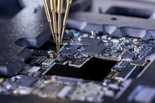
In-circuit testing (ICT) uses electrical contact with accessible points to check selected features of an assembled board. Depending on the tester and test program, measurements can help identify certain opens, shorts or component-value issues.
A bed-of-nails fixture uses spring-loaded probes positioned for a particular board. Once the fixture and program are prepared, multiple test points can be contacted during a test cycle. This can make a dedicated fixture attractive for a stable design with repeat production, although the upfront development and fixture cost must be considered.
The fixture cannot measure every feature automatically. Coverage depends on which nets and components are accessible, the test equipment, the program and the agreed fault model. An unprobed net or a function that requires a separate operating sequence may need another test method.
Manufacturing defect analysis (MDA) is a related approach that focuses on selected assembly defects and electrical measurements. The checks available under an MDA or ICT plan depend on the equipment and program; ask for the expected scope rather than relying on the name alone.
Flying Probe Testing
A flying probe tester moves probes to programmed contact locations on the assembly. It avoids the need for a dedicated bed-of-nails fixture, although the board still needs suitable support, accessible contact points and a test program.
Because probe positions are controlled by the program, this approach can be useful for prototypes, smaller batches or designs that may change. The probes must travel between measurements, so test time can become a consideration as the number of checks and boards increases.
Flying probes can also perform in-circuit measurements. The practical comparison is therefore between different ways to access and test the circuit, not a rule that flying probe and ICT are unrelated. Keysight describes both approaches.
| Consideration | Bed-of-nails fixture | Flying probes |
|---|---|---|
| Board contact | Dedicated probes positioned for the board | Moving probes visit programmed locations |
| Initial preparation | Fixture and test program must be developed | Program and suitable board support are needed |
| Design changes | A change affecting access may require fixture and program changes | Probe positions and the program can be revised, subject to access |
| Test time | Can contact multiple points during a cycle | Probe movement between measurements affects cycle time |
| When to evaluate | Stable designs and repeat quantities where fixture cost can be justified | Prototypes, smaller runs or designs with expected changes |
These are planning considerations, not universal quantity thresholds. Board density, access, required coverage and the test program can change the result for either approach.
Compare the cost across the expected build
A fixture has an upfront cost; both approaches also require engineering and a per-board test cycle. For an initial comparison, include program development, fixture or setup work, the estimated cycle time, and any expected revisions or retests. Ask the test provider what each quotation includes.
For illustration only, suppose a fixture and its setup cost $1,000, with a test cost of $1 per board. If an alternative has no dedicated fixture charge and costs $3 per board, the direct comparison is $1,000 + $1 × quantity versus $3 × quantity. The two totals are equal at 500 boards. Below or above that quantity, the cheaper option changes under those assumptions.
This example is not a GreatPCB price or a recommendation to select a method on cost alone. Coverage, contact access, changes to the design and the consequences of a missed defect can change the decision. A fixture may also be modified for some revisions; it does not necessarily need to be discarded after every design change.
Functional Testing (FCT)
Functional testing checks whether specified parts of the assembled board operate under defined conditions. A test might apply power, verify a voltage, send a command through an interface or check that an output responds within an agreed range.
Unlike a general visual inspection, a useful functional test needs a procedure. That procedure should identify the board revision, firmware, power supply, connections, inputs, expected responses and pass/fail limits. Some products also need a fixture, a programmed test application, a load or a simulated connection to another system.
Example: A Functional Test for a Controller Board
Consider a controller board with a communication port. A defined functional test could verify that the board starts, draws current within an agreed range and responds to a specified command. Passing those steps confirms those conditions; it does not automatically validate every software feature, temperature range or lifetime requirement.
For a simple hypothetical procedure, the product owner specifies a 12 V input, a permitted idle current of 80–120 mA, and a required response to a communication command. The operator connects the approved supply and interface, applies power under the specified setup, measures idle current and sends the command. A result of 105 mA meets the illustrative current limit; a missing response still fails the communication step. The values are examples, not limits for your design or GreatPCB service specifications.
Match the Test Setup to the Product
The test setup matters as much as the list of functions. A motor controller checked with a resistive load, for example, has not necessarily been evaluated against the transient behavior of the intended motor. Where that behavior matters, agree whether the test needs a representative load or a separate validation step.
Record the firmware version and the expected response for each step. An onboard self-test can provide useful information, but it may not exercise every external interface or operating mode. Decide which results need an independent measurement and which conditions belong to product qualification rather than routine production testing.
Agree on the Procedure Before Production
Agree who supplies the test procedure, equipment, fixtures and firmware, and how failures and retests will be handled. Altium’s testing overview explains why functional requirements should be communicated to the manufacturer early.
How to Choose a PCB Assembly Test Plan
Visual / AOI
X-ray where needed
ICT / flying probes
Functional test
Start with the failures that matter to the product, then work backward to the inspection or test that can find them. Volume, package type, access, available documentation and the consequences of a missed defect all influence the plan.
A Prototype with a Changing Design
When a design is still being revised, a dedicated fixture may need changes as the layout changes. Review visible assembly features and discuss electrical access and functional checks for the prototype. Flying probes can be worth evaluating where suitable contact points are available.
If the product has not yet completed bring-up, separate a manufacturing defect from a design or firmware issue. A clear test procedure and a way to record the failure make that distinction easier.
For example, if the board powers up but does not answer an interface command, the team can first check the supplied firmware and connector setup, then follow the agreed diagnostic procedure. A failed command alone does not identify whether the cause is soldering, a component, firmware or the test connection.
An Assembly with BGA or QFN Components
Optical inspection can examine many visible features, but it cannot see through a package to inspect concealed solder joints. Identify the packages or joints that need X-ray review and agree on the inspection criteria. Then consider what electrical or functional tests are needed to assess the circuit itself.
A Stable Product Built Repeatedly
For repeat orders, compare the one-time work of developing a fixture and test program against the time required to test each board. The decision depends on expected production quantities, revision stability, coverage and access—not on quantity alone.
A Board with Critical Functions
If a board must control a motor, communicate with a host or deliver a defined output, name the functions and conditions that need verification. A simple power-on check may be useful, but it does not substitute for the specific functional procedure or product qualification required by the project.
Inspection, ICT, flying probe and FCT may be combined where appropriate. The selected checks, sampling, acceptance criteria and reports should be agreed for the order; the number of methods alone does not define the quality of a test plan.
Design for Testability and Fixture Planning
Allow a clear path to the test pad.
Check nearby components and board support.
Testability is easier to address before the layout is released. Once components and enclosures limit access, adding a reliable probe contact can require a board revision or a different test approach.
Plan Access to the Signals You Need
Identify the nets, power rails, grounds and interfaces needed for the intended checks. A test point can provide a known location for a probe, but its usefulness depends on the surrounding components, solder mask, board geometry and the type of test.
For example, a pad may exist in the CAD data but be blocked by a connector or too close to a tall component for the intended probe. Review physical access on the assembled board, not only the unpopulated layout.
Avoid adding arbitrary test points to sensitive signals without engineering review. High-speed or RF structures may require a measurement approach that considers signal integrity, connectors and the test setup.
Allow for the Fixture and Board Support
A fixture needs a repeatable way to locate and support the assembly. Probe contact, component clearance and support positions all matter. Excessive or uneven force can bend a board or stress solder joints; the fixture design should suit the board thickness, size and component layout.
Agree the required test-point dimensions, spacing, edge clearance and board support with the fixture or test equipment provider for the specific design. There is no single dimension that can be assumed to fit every tester and assembly. Altium’s ICT design checklist provides further context for early testability planning.
Define Coverage Before Releasing the Design
Provide the board revision, netlist and proposed test points for review. Ask which required nets are accessible, which checks cannot be performed and whether any additional access or alternative method is needed.
Record design changes that affect test points or component placement. A new board revision may also require changes to the fixture, program, functional procedure or acceptance limits.
Test access is not the same as fault coverage. A reachable pad gives a probe a contact location; it does not by itself show that a particular open, component fault or functional failure will be detected. When a coverage percentage is requested, define the denominator, fault types, test conditions and any exclusions with the test provider before comparing figures.
Place test points on a common side where practical, but verify this against the actual assembly and fixture. A via can sometimes provide access, depending on its finish, construction and probe design; do not assume every via must be filled or that every via is suitable. Probe type, pad size and spacing need project-specific review.
Use Test Results to Improve the Next Build
When a board fails, record the board identifier and revision, test step, measured result, limits and disposition. Separate a confirmed defect from a probe-contact problem or an unverified test setup; repeat the agreed check after authorized repair or correction.
For repeat builds, grouping confirmed failures by component, location or process stage can reveal a recurring issue. Discuss findings with the engineering and production teams so that an assembly process or test program can be reviewed. The format and availability of records should be agreed for the order.
What to Provide for a Testing Quote
The right documents depend on the project and test method. The following information helps establish the scope before a quotation or production release:
| Information | Details to provide or discuss |
|---|---|
| Assembly and quantity | Board part number and revision, build quantity, expected repeat orders and delivery requirements |
| Manufacturing files | BOM, assembly drawings, component placement data, board files and available netlist |
| Inspection requirements | Critical packages or joints, required methods, agreed acceptance criteria and sampling |
| Electrical access | Test-point locations, accessible nets, constraints and any existing fixture or program |
| Functional procedure | Power and connections, inputs, expected outputs, limits, sequence and test environment |
| Firmware and equipment | Firmware version, programming files, interface equipment, loads, software and responsibilities |
| Records and failure handling | Required results, traceability, disposition of failures, repair authorization and retest requirements |
If the test procedure is not yet complete, identify the functions and risks that matter most. GreatPCB can review the available project information with you and clarify the proposed inspection and test scope. Confirm the actual services, fixture arrangements and deliverables in the quotation.
Frequently Asked Questions
Is AOI enough for BGA solder joints?
AOI checks features visible to its cameras. BGA solder joints are underneath the package, so they may require X-ray inspection when the project calls for assessment of those hidden connections. Agree the required locations and criteria for the inspection.
What is the difference between in-circuit testing and functional testing?
In-circuit testing makes electrical measurements at accessible points to check selected components or connections. Functional testing operates the board according to a defined procedure and checks specified responses. The two can complement each other; neither automatically covers every possible defect or operating condition.
When is flying probe testing a good choice?
It is worth considering when a design is changing, the order quantity is modest or a dedicated fixture is not justified. The test points must still be accessible, and the program and cycle time should be reviewed against the project’s needs.
Can a PCB assembly be tested without a custom fixture?
Some checks can be performed without a board-specific bed-of-nails fixture. Examples may include visual inspection, AOI, selected flying-probe measurements or a functional test through existing connectors. The available options depend on the design, access and agreed procedure.
Who provides the functional test procedure and firmware?
The product owner typically defines the required functions and acceptance limits. The parties should agree who supplies or develops the procedure, firmware, test equipment and fixture before production. Availability and responsibility depend on the project.
Does a passed functional test guarantee long-term reliability?
No. It confirms performance only under the conditions and limits included in that test. Environmental, endurance or other qualification tests may be needed if the product requirements call for them; their scope should be specified separately.
Discuss Your PCB Assembly Testing Requirements
Tell us about your assembly, production quantity, component packages and the checks you need. Our team can review the manufacturing and test requirements with you and help clarify the scope for your quotation.