
Through-Hole and Mixed Technology PCB Assembly
A board can need compact surface-mounted ICs and components that pass through the PCB, such as connectors, relays or larger capacitors. Building both on the same assembly requires a coordinated plan for placement, soldering, inspection and testing.
GreatPCB provides through-hole and mixed-technology PCB assembly, bringing SMT placement and leaded component assembly together for prototype and production projects. Our services can include PCB fabrication, component sourcing and inspection, helping you coordinate the complete assembly from your design files to finished boards.

Through-Hole AssemblyLeaded connectors, power components and other parts
Mixed TechnologySMT and through-hole components on the same board
PCB + Component SupportFabrication, sourcing and coordinated assembly
Inspection & TestingChecks planned around the requirements of the build
What Is Mixed Technology PCB Assembly?
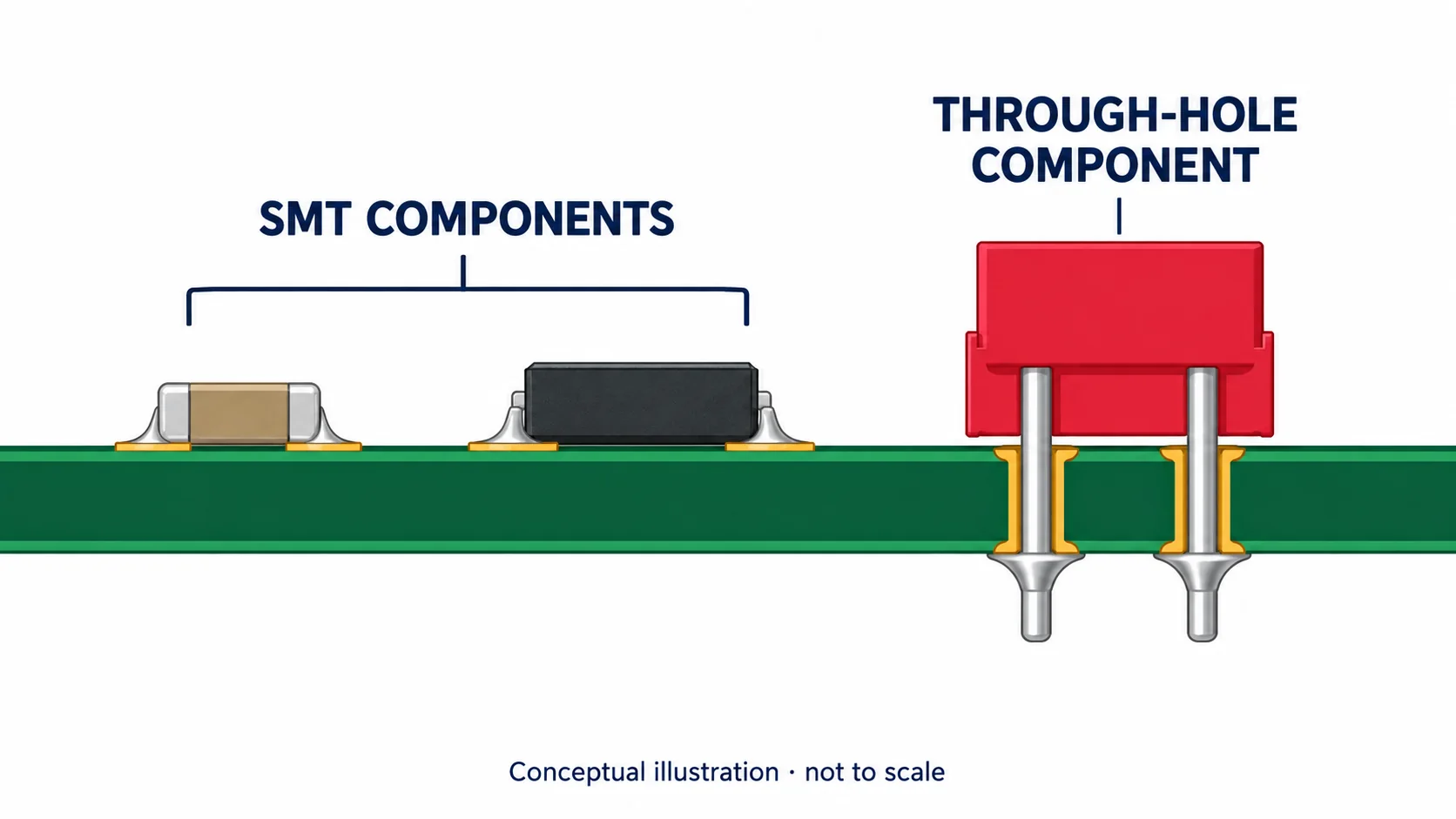
Mixed technology assembly combines surface-mount technology (SMT) and through-hole technology (THT) on the same printed circuit board. SMT components are mounted to pads on the board surface. Through-hole components have leads that pass through holes and are soldered to form the required connections.
The distinction matters during production. A component’s package determines how it is positioned, how its joints are formed and which parts of the board must be accessible. A mixed assembly therefore needs more than two separate lists of components: the processes must work together without compromising parts that are already installed.
Explore our complete PCB assembly services or learn more about our PCB assembly factory.
Through-Hole Components in a Mixed Assembly
Through-hole packages are still used for connectors, terminals, relays, transformers, switches, capacitors and other leaded components. A design may select them for component availability, mechanical mounting, electrical requirements or compatibility with an existing product.
The right package depends on the whole design. A connector subject to repeated use may need mechanical support; a large component may need space for insertion and handling. Neither the package type nor a solder joint alone guarantees the finished product’s reliability.
| Component example | Assembly consideration | What to clarify |
|---|---|---|
| Connectors and terminal blocks | Orientation, seating and access to the leads | Mating direction, height, mechanical support and nearby parts |
| Relays and switches | Correct pin pattern and installation position | Footprint, polarity where relevant, height and clearance |
| Leaded capacitors and power components | Lead spacing, thermal mass and heat sensitivity | Orientation, required standoff and soldering constraints |
| Transformers and inductors | Weight, seating and access around multiple leads | Mechanical support, allowed process exposure and finished height |
Sharing the component drawings and assembly requirements helps the team plan part placement, handling and soldering before production.
How SMT and Through-Hole Assembly Work Together
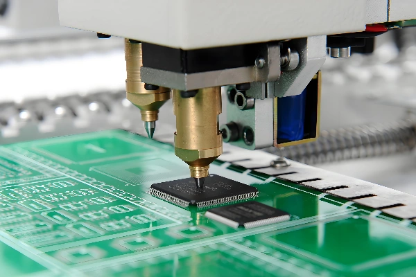
One possible sequence is to print solder paste, place SMT components and reflow them, then insert and solder the through-hole parts before final inspection. Some designs require a different order or additional steps. Component temperature limits, board layout, both-side placement and the chosen soldering process can change the sequence.
A Typical Mixed-Assembly Workflow
| Stage | What happens | What the team checks |
|---|---|---|
| 1. Design review | Review the BOM, board files and assembly drawing | Hole-to-lead fit, component orientation, access and board support |
| 2. SMT assembly | Apply solder paste, place surface-mounted parts and reflow | Placement and solder joints before the next operation |
| 3. Through-hole insertion | Place leaded components into their assigned holes | Seating, polarity, pin alignment and handling of tall or heavy parts |
| 4. Through-hole soldering | Apply the soldering process selected for the board | Access, nearby parts, heat exposure and joint formation |
| 5. Inspection | Inspect assembly features and accessible solder joints | Missing or reversed parts, solder bridges, wetting and seating |
| 6. Testing and delivery | Perform the checks specified for the order and prepare boards for shipment | Functional test setup, acceptance limits and packaging requirements |
The sequence and inspection points are adapted to the component mix and production requirements. GreatPCB’s PCB assembly factory brings SMT/THT assembly together with inspection systems and project-specific testing.
Review the Board Before Assembly
The BOM, assembly drawing and board data should agree on the component reference, footprint, orientation and revision. Check which components are SMT, which have leads through the board and whether the finished assembly has height or handling restrictions.
For example, a tall connector near a row of small SMT parts may limit access to its leads. Identifying that conflict during review gives the assembly team a chance to discuss the process or layout before the parts are installed.
Coordinate Soldering and Inspection
SMT and through-hole joints may experience more than one heating operation. Review the exposure permitted by the components, the board and the solder system when planning the sequence. A protective fixture, an alternative process or a change in order may be considered where appropriate.
Inspection points should match the production plan. The team can review SMT placement and visible joints, then check the through-hole component seating, orientation and relevant soldered connections. Findings should be resolved before subsequent work makes access more difficult.
Choosing a Through-Hole Soldering Method
Through-hole joints can be soldered by hand, by wave soldering or by a selective process. The right approach depends on the board layout, component requirements and production quantity.
| Method | How it works | Useful considerations |
|---|---|---|
| Hand soldering | An operator applies heat and solder to individual joints | Access, operator technique and the number of joints affect planning; can be useful for selected or difficult-to-process parts |
| Wave soldering | The solder side passes over a flowing wave of molten solder | A board with many suitable joints may benefit from a repeatable process; bottom-side parts, orientation, masking and fixtures need review |
| Selective soldering | A programmed system applies solder to specified locations | Localized soldering can help with mixed layouts; nozzle access, programming, support and cycle time still matter |
Wave vs. Selective Soldering
Wave soldering exposes the relevant side of the board to a solder wave. Selective soldering directs solder to specified locations. Neither method is automatically correct for every mixed assembly: the positions of nearby parts, the required access, the thermal plan and tooling all affect the decision.
For a connector surrounded by small SMT components, the assembly plan must account for access to each through-hole joint and protection of nearby parts. Selective soldering uses a programmed path to apply solder to selected joints, while wave soldering can process multiple suitable joints as the board passes over the solder wave.
For a row of connector pins, a selective-solder program may move along the row; individual joints may instead be soldered separately when their positions or nearby parts make that approach more suitable. The choice depends on access and the equipment, and both approaches require a suitable process plan.
How the Choice Affects the Quote
Compare the number and location of joints, board-side clearance, tooling and expected order quantities. A fixture or program can add setup work, while soldering individual joints can add labor or cycle time. For repeat builds, discuss the anticipated total quantity and design revisions as well as the first order; there is no universal quantity at which one method becomes cheaper.
| Cost driver | Effect on the assembly plan |
|---|---|
| Number of through-hole joints | More individual joints can increase insertion and soldering time per board |
| Joint location and nearby SMT parts | Crowded areas may need additional access, masking or localized soldering |
| Fixtures and programming | A setup cost may be spread across the boards built with the same tooling and program |
| Order quantity | Higher quantities spread fixed setup costs across more boards |
| Design revisions | A changed layout can require adjustments to fixtures, programs or work instructions |
| Inspection and test scope | Additional checks, fixtures or documentation add work to the order |
Example: Comparing Setup and Per-Board Cost
The following example shows how quantity affects a process decision. The dollar amounts are illustrative assumptions, not GreatPCB prices or quotations, and cover only the compared soldering work.
| Assumed cost | Process A | Process B |
|---|---|---|
| One-time setup | $0 | $120 |
| Soldering cost per board | $0.55 | $0.25 |
| Total for 100 boards | $55 | $145 |
| Total for 1,000 boards | $550 | $370 |
Under these assumptions, Process B’s $120 setup is offset at 400 boards: $120 ÷ ($0.55 − $0.25). The result changes with joint count, labor, tooling, revisions and repeat orders; the full assembly quote also includes other project costs.
Design Considerations for Mixed Assemblies
Hole, Lead and Component Fit
The lead must fit its intended hole, and the component must seat at the required position. Review the component drawing and finished-hole requirements together; a hole size from an unrelated project is not a universal design rule.
For polarized components and connectors, an assembly drawing should make orientation clear. Note any required height, standoff, lead forming or mechanical support instead of relying on the footprint alone.
Access and Clearance
A joint needs enough physical access for the intended soldering and inspection method. Nearby SMT components, tall connectors and board edges can limit a nozzle, soldering iron, fixture or inspection view.
Where a board needs a carrier or solder pallet, review the support areas and any openings early. A wave-solder pallet is not required for every design, and a selective process may still require board support or a fixture.
Example: A Connector Row Near Bottom-Side SMT Parts
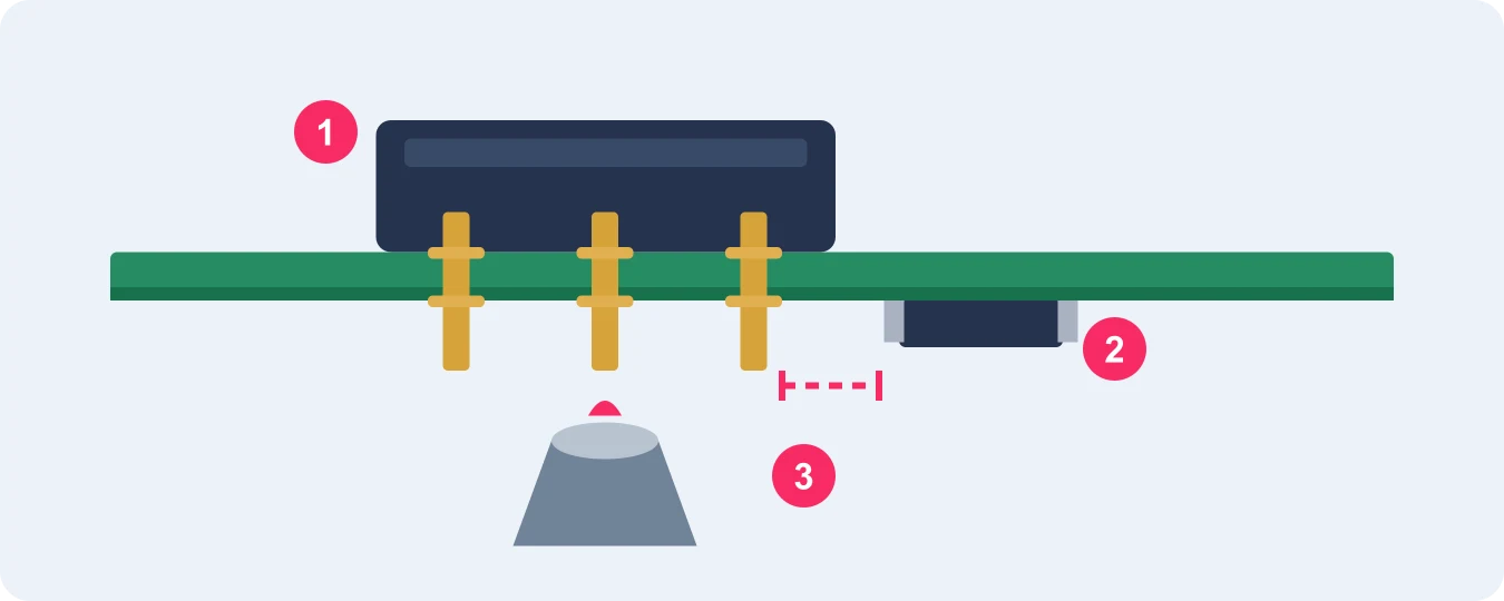
Conceptual illustration; not to scale.
Consider a control board with a through-hole terminal block and small SMT components on the solder side. Before choosing a process, review the connector drawing against the footprint and check the space around the pins and nearby components. The soldering tool or nozzle needs access without disturbing adjacent parts; for wave soldering, the team should also evaluate whether those parts need protection.
Check how the board will be supported and whether the connector can stay seated and correctly oriented during soldering. If large copper areas or substantial pins affect heating, the process must account for them while respecting component temperature limits. After soldering, inspect accessible joints for bridging and other visible issues under the agreed criteria.
Thermal and Process Sequence
Consider how the soldering sequence affects parts already installed. Large copper areas and heavy leads can draw heat away from a joint; heat-sensitive components may restrict the allowable process. The assembly team should review the relevant material and component documentation for the proposed operation.
Through-hole reflow, also called pin-in-paste, uses solder paste to form joints for compatible leaded components during reflow. It requires components that can withstand the reflow profile and a design that supports the required paste volume and hole fill. Package geometry, board thickness and the rest of the assembly all affect whether the approach is suitable.
Inspection and Testing
After insertion and soldering, inspection may address component presence, orientation, seating and visible solder-joint features. The applicable drawing and agreed acceptance criteria determine what is checked and how an issue is handled.
Visible Joints and Hidden Barrel Fill
Visible solder around a lead can be inspected for features such as bridging or incomplete wetting. The surface appearance alone does not establish the solder fill inside a plated hole. Where internal fill is important, inspection and process controls should be selected to match the joint and the project’s acceptance criteria; X-ray can help assess hidden features when appropriate.
An electrical or functional test answers a different question from visual inspection. If the project needs checks beyond the visible assembly, define the test procedure, points of access and pass/fail limits in advance. See PCB Assembly Testing and Inspection for a discussion of AOI, X-ray, electrical and functional checks.
If a board fails a check, the disposition, repair authorization and retest should follow the project agreement. Specify any reporting or traceability requirements before production.
Frequently Asked Questions
Can SMT and through-hole components be assembled on the same board?
Yes. A mixed-technology board uses both surface-mounted and through-hole parts. Its process sequence must account for component placement, soldering access and the permitted thermal exposure.
Is selective soldering always required for a mixed board?
No. The choice depends on the layout, part requirements, quantities, available equipment and possible tooling. Hand, wave or selective soldering may be considered according to the project.
Can you assemble a board that uses only through-hole components?
Discuss the component types, board construction and quantity with GreatPCB. The team can review the order and confirm the appropriate assembly scope and available soldering method.
Can customers supply some of the components?
Material responsibility should be agreed for the order. Identify customer-supplied parts, quantities, packaging and any handling requirements so that the team can review the proposed sourcing and assembly scope.
What information helps the team prepare a quote?
Provide the board design files, BOM and assembly drawing with matching revisions, the quantities and any customer-supplied components. Include placement and polarity requirements, special handling, inspection criteria and functional test instructions where applicable. The team can then identify missing information and discuss the proposed process and any tooling.
Is functional testing included automatically?
Functional testing is planned around the product. Provide the test procedure, firmware, equipment or fixture requirements, and acceptance limits so the required checks can be included in the project scope.
Discuss Your Through-Hole or Mixed Assembly Project
Tell us about the board, component packages, quantity and inspection requirements. GreatPCB can review the proposed PCB fabrication, sourcing and assembly scope and clarify the requirements for a quotation.