Technical
Assembly
Technical
Assembly
BGA, also known as Ball Grid Array packaging technology, is a high-density surface mount packaging technology. At the bottom of the package, the pins are spherical and arranged in a grid-like pattern, hence the name BGA.

What are the advantages of BGA packaging? How does it differ from other packaging methods?
1. Pin Layout and Density
Traditional pin packaging (such as DIP, SOP, etc.) usually arranges the chip pins on two or four sides of the package. In contrast, BGA packaging distributes the chip pins across the entire bottom surface and connects them using spherical solder balls. This layout allows BGA packaging to achieve higher pin density, enabling a reduction in volume to one-third while maintaining the same memory capacity. This makes it suitable for high-performance chips with a large number of pins, such as processors and graphics chips.
2. Manufacturing Process
Traditional pin packaging manufacturing processes often require manual pin alignment and soldering operations, which are time-consuming and prone to errors. In contrast, BGA packaging typically uses automated equipment for manufacturing, eliminating the need for manual pin alignment and soldering. This makes the BGA packaging process more efficient, reliable, and cost-effective.
3. Thermal Performance
Traditional pin packaging usually lacks special thermal design. BGA packaging, however, often features a metal bottom, with a larger contact area that helps in better heat dissipation. Additionally, the connection of the chip and substrate through solder balls forms a strong thermal conduction path, allowing the heat generated within the chip to dissipate more effectively to the external environment. Therefore, compared to other packaging methods, BGA packaging excels in thermal performance.
4. Signal Transmission and Interference
In traditional pin packaging, the pins connect the chip and substrate through long and narrow wires, which are susceptible to signal noise and crosstalk. In contrast, BGA packaging connects the chip and substrate through solder balls, resulting in shorter and more stable signal transmission paths. This effectively reduces the risk of signal interference and provides more reliable signal transmission.
5. Mechanical Stability
Due to its superior performance, BGA packaging is particularly suitable for high-density, high-power chips such as microprocessors and graphics chips. It is widely used in communication equipment, computers, automotive electronics, consumer electronics, industrial control, and instrumentation.
BGA Packaging Process Flow
1. Wafer Thinning
Wafer thinning is achieved by grinding the back of the wafer with a grinding wheel at high speed. This process also requires water cooling and cleaning to prevent heat accumulation and debris buildup. If the chip needs to be thinned to a certain thickness, it is polished based on the product type to reduce internal stress. After thinning, the wafer surface film is removed using tape, followed by thickness measurement and quality inspection.
2. Chip Cutting
After wafer thinning, the wafer is fixed on a metal ring using blue tape for cutting into individual chips. The main chip cutting methods are blade cutting and laser cutting. Blade cutting uses a circular blade to completely cut along the wafer dicing path, dividing the wafer into individual chips that are orderly arranged on the blue tape. Laser cutting uses the energy of a laser beam to evaporate the material along the dicing path, separating the wafer into individual chips. As IC wafer processes advance to below 10nm, more low-k materials are used, and laser cutting can meet the needs of non-contact cutting, narrow cutting width, and high cutting quality.
3. Chip Mounting
Chip mounting involves fixing the chip onto the substrate using materials such as silver paste or DAF film, based on the design drawing. The main purpose is to secure the chip and conduct heat from the chip.
4. Plasma Cleaning
Plasma cleaning before wire bonding uses ionized argon ions, electrons, and active groups to volatilize contaminants on the substrate and chip surface, which are then removed by a vacuum system. This achieves surface cleaning, enhancing the bonding strength during wire bonding. Plasma cleaning before encapsulation works similarly, using high-energy argon and oxygen ions to clean surface contaminants and carbon residues, activating the substrate surface to increase bonding strength between the PCB and encapsulation material, improving product reliability.
5. Wire Bonding
Wire bonding is a crucial step in packaging, where wires (gold, copper, or silver alloy) are bonded to the aluminum pads on the chip and the metal pads on the substrate, achieving electrical connection. The following image shows the SEM image after BGA wire bonding.
6. Encapsulation
Encapsulation involves melting the encapsulation material at high temperatures into a low-viscosity liquid, which is then injected into the mold cavity. The encapsulation material’s internal epoxy resin cures with the help of hardeners and coupling agents, completing the encapsulation.
7. Post-Curing
Post-curing involves baking the encapsulated material at high temperatures to complete the reaction of the encapsulation material, stabilizing the epoxy resin molecular structure, increasing encapsulation hardness, and relieving internal stress.
8. Marking
Marking involves ink printing or laser engraving on the front of the chip to label the product name, production date, and other information for product identification and traceability, as shown below.
9. Ball Placement
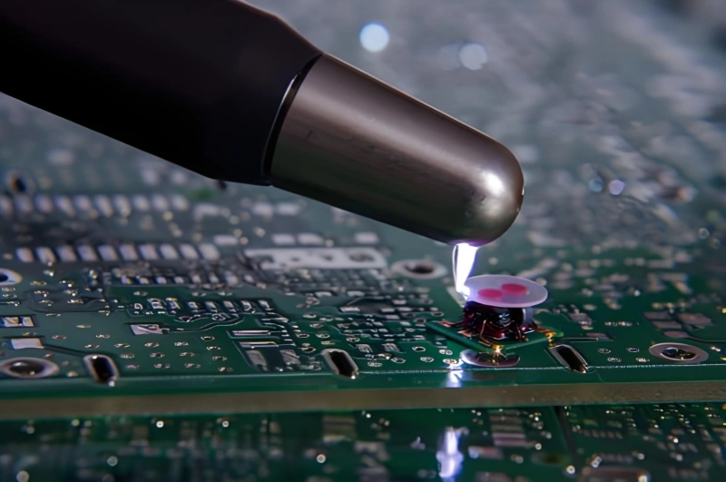
This is a special process in BGA packaging where solder balls are placed on the solder pads (NiAu or copper OSP) on the back of the substrate. Solder paste is applied, and the balls are reflowed in an oven to form a eutectic with the solder pads, securing the balls to the substrate after cooling. The reflowed solder balls become the I/O pins of the BGA package, connecting the chip to external circuits. The following image illustrates the ball placement process.
10. Singulation
Before singulation, all processes are carried out on a strip basis. This step involves separating the BGA substrate strip into individual BGA chips through cutting or stamping, forming the final product.
BGA Fan-Out Considerations
1. 1.0mm BGA
- Single trace between vias: Use 10-22 mil via, 6 mil trace width, 5.5 mil trace-to-via clearance.
- Single trace between vias: Use 8-18 mil via, 6 mil trace width, 7.5 mil trace-to-via clearance.
- Two traces between vias: Use 8-18 mil via, 4 mil trace width, 4 mil trace-to-trace, 4.6 mil trace-to-via clearance. For differential pairs, use 4/4 mil spacing within the BGA, changing to differential spacing outside the BGA.

2. 0.8mm BGA
- Only one trace between adjacent vias: Generally use 8-18 mil via, 5 mil trace width, 4 mil trace-to-trace, 4.24 mil trace-to-via clearance.
3. 0.65mm BGA
- Use 8-16 mil via, no traces between adjacent vias, adjust fanout.
- Use 8-16 mil via, traces between adjacent vias, inner layer pad reduction, 4 mil trace width, 5.3 mil trace-to-via clearance (Note: No traces on the same layer with via leads).
- Use 8-14 mil via, 3.5 mil trace width, 4 mil spacing, 4 mil trace-to-via clearance. This method can follow standard BGA routing but is challenging to manufacture.


