HDI PCB
FR4 standard
Assembly
What is HDI PCB?
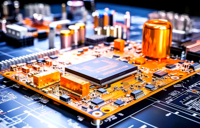
HDI PCB stands for High Density Interconnect Printed Circuit Board. Unlike traditional PCBs that rely on mechanical drilling, HDI PCBs use laser drilling technology, which allows for much smaller hole diameters, typically in the range of 3-6 mils, and line widths of 1.8-4 mils. This advancement significantly increases the density of the circuits within the same unit area, providing more efficient and compact designs. The emergence of HDI technology has propelled the development of the PCB industry by enabling the integration of denser components like BGAs and QFPs.

How Does HDI PCB Differ from Traditional PCBs?
- Size and Weight: HDI PCBs are compact and lightweight. They are constructed by repeatedly stacking layers, resulting in a buildup multilayer board (BUM). This construction method offers the advantages of being lighter, thinner, shorter, and smaller compared to traditional boards.
- Manufacturing Process:
- Microvias: HDI boards contain blind and buried microvias, typically less than 150 microns in diameter, which require high precision and cost-effective manufacturing techniques.
- Line Width and Spacing: HDI PCBs feature fine line widths and spacings, generally not exceeding 76.2 microns.
- High Pad Density: HDI boards have a high density of solder pads, exceeding 50 per square centimeter.
- Thin Dielectric Layers: The dielectric layers between HDI PCB layers are often thin (80 microns or less) and require uniform thickness, especially for high-density boards with impedance control.
- Electrical Performance: HDI PCBs not only allow for more compact designs but also enhance electronic performance and efficiency. The increased interconnect density improves signal integrity and reliability, while also mitigating issues such as RF interference, EMI, ESD, and thermal management.
- High Requirements for Via Filling: The production of HDI PCBs involves high standards for via filling. Poor via filling can result in significant quality issues such as uneven board edges, non-uniform dielectric thickness, and irregular pad surfaces.
Applications of HDI PCBs
HDI PCBs are predominantly used in high-end electronic devices such as communication equipment, computers, medical devices, and automobiles. Their high density, reliability, and superior performance make them critical in these applications.
Structure and Classification of HDI PCBs
- Blind Vias: These can be categorized into stacked and staggered vias.
- Via Filling: All blind vias are typically filled to ensure reliability and performance.

HDI PCB Manufacturing Process
Material Cutting -> Drilling -> Copper Plating -> Laser Drilling -> Desmear -> Electroless Copper Deposition -> Pattern Plating -> Etching -> Lamination -> Surface Treatment -> Solder Mask Application -> Silkscreen Printing -> Electrical Testing -> Final Inspection

About HDI PCB Manufacturers
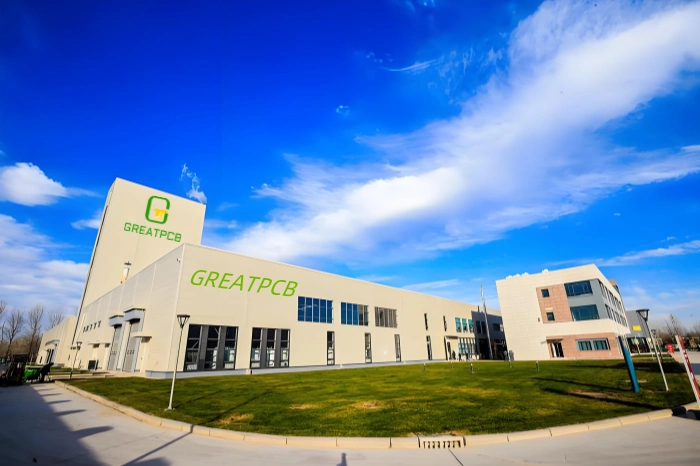
To develop and enhance the capability and strength required for producing high-density interconnect (HDI) PCBs, Greatpcb has been diligently striving for over a decade. Today, Greatpcb boasts a comprehensive production system and state-of-the-art automated equipment, ensuring that all product quality inspections adhere strictly to IPC Class 2 standards. With years of technical accumulation and continuous investment in equipment, Greatpcb is equipped to provide high-quality HDI PCB products, catering to the demands of various high-end electronic devices.


