ENIG vs HASL: Which Is Better for PCB Assembly?

Selecting the right PCB surface finish changes your assembly yield, long-term reliability, and total cost. ENIG vs HASL is the most common trade-off engineers face. You want the solderability and protection your board needs—without paying for unnecessary complexity. This article gives you factory‑proven comparisons: flatness numbers, real shelf‑life data, pitch limits, and cost per panel. You will learn exactly when HASL is the smart choice and when ENIG saves you from field failures. We cover IPC standards, black pad prevention, and mixing finishes for cost optimization. Let’s solve your surface‑finish decision together.
What is HASL (Hot Air Solder Leveling)?
HASL is one of the oldest and most widely used PCB surface finishes. The process dips the finished circuit board into a bath of molten solder—either traditional tin‑lead or, for RoHS compliance, a lead‑free alloy such as SAC305. High‑pressure hot air knives immediately blow off excess solder, leaving a coating only on the exposed copper pads.
The result is a solderable layer that protects the copper and provides a reliable soldering surface for assembly. Lead‑free HASL operates at around 260°C, while the older leaded version works at lower temperatures.
Advantages of HASL
- Low cost – HASL is the most affordable finish. For a standard 2‑layer FR4 board, the adder is typically $0.02–0.04 per square inch in volume. If your project is large and budget‑sensitive, this keeps the PCB cost down.
- Excellent solderability (when fresh) – HASL‑finished pads readily accept solder. The tin‑based coating creates a strong bond with the assembly solder during reflow or wave soldering.
- Robust for through‑hole components – The thick solder coating on plated holes provides good solder volume during assembly, making it ideal for connectors, headers, and discrete leaded parts.
- Fast process – HASL does not need an extended plating line. Most factories can apply it in‑line and turn boards the same day, shortening overall lead time.
Disadvantages of HASL
- Uneven surface – The hot air leveling leaves a meniscus of solder on each pad. Flatness deviation can range from 5 µm to 25 µm across a single BGA pad. This variability creates co‑planarity problems when placing fine‑pitch parts.
- Not suitable for fine‑pitch SMT – Components with a pitch below 0.8 mm (like 0.5 mm QFPs, BGAs, or QFNs) often experience solder bridging or open joints because the pad surface is not flat.
- Thermal stress on the board – Dipping the entire PCB into molten solder subjects the laminate to a thermal shock. Thin boards (<0.8 mm) or low‑Tg materials (Tg < 130°C) may warp or suffer pad lifting.
- Limited shelf life – HASL coatings oxidize over time. While fresh boards are highly solderable, after 3–6 months in standard storage (30–60% RH, 20–25°C), wetting force can drop below 95% of the original value. This slowdown affects first‑pass assembly yield.
- RoHS considerations – Leaded HASL is non‑RoHS compliant and can only be used in exempt applications. Lead‑free HASL meets RoHS, but it still has flatness and thermal issues.
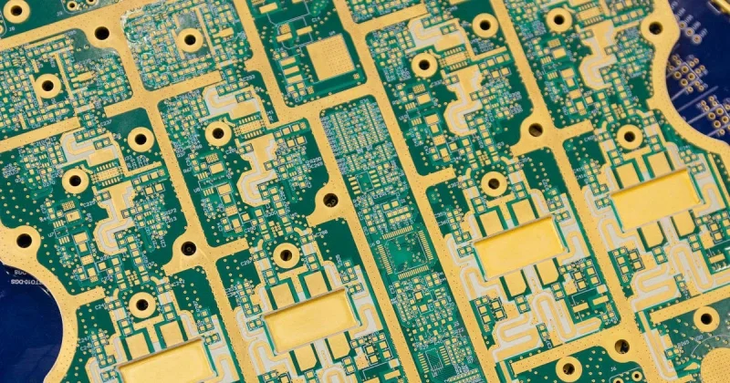
What is ENIG (Electroless Nickel Immersion Gold)?
ENIG is a two‑layer metallic coating applied through a chemical process, not electroplating. First, an electroless nickel layer (typically 3–6 µm thick) is deposited directly on the copper pads. Next, a thin immersion gold layer (0.05–0.12 µm) is deposited through a displacement reaction on top of the nickel. No external electrical current is used.
The nickel acts as a diffusion barrier—it prevents copper from migrating into the gold and creating brittle intermetallics. The gold protects the nickel from oxidation and provides a pristine, solderable surface.
Advantages of ENIG
- Perfectly flat surface – ENIG’s deposition is chemical and self‑limiting, so the surface follows the underlying copper with a flatness deviation of less than 1 µm. This makes it mandatory for high‑density boards using BGAs with 0.5 mm pitch or smaller.
- Excellent for fine‑pitch components – The consistent planarity eliminates solder bridging and open circuit risks on QFN, BGA, and 0201 chip packages. ENIG meets the coplanarity requirements of IPC‑7095 for BGA assembly.
- Long shelf life – When stored in vacuum‑sealed packaging at 20–25°C and 30–60% relative humidity, ENIG boards maintain full solderability for 12 months. This is critical if your boards will sit in inventory before assembly.
- Oxidation resistance – The gold layer is chemically inert, so pads do not tarnish. Even after multiple reflow cycles or long storage, wetting remains consistent.
- Superior for high‑frequency circuits – The smooth nickel‑gold surface reduces skin‑effect losses and minimizes impedance discontinuities in traces carrying signals above 5 Gbps.
- Good for multiple reflow cycles – ENIG withstands several thermal cycles without losing integrity, which helps when a board undergoes double‑side assembly plus rework.
Disadvantages of ENIG
- Higher cost – The material and process add about $0.08–0.15 per square inch to the board cost compared to a bare copper finish. For large panels, this increase is measurable. However, the cost delta shrinks as batch sizes grow because plating line efficiency improves.
- Black Pad risk (phosphorus‑enriched nickel) – This is the most well‑known ENIG defect. When the immersion gold bath is not tightly controlled, the nickel surface can corrode unevenly, leaving a phosphorus‑rich layer. During soldering, this layer forms a brittle Ni3Sn4 intermetallic that fractures easily. The result is an intermittent or open solder joint. Modern process control has largely solved this issue, but the risk remains with uncalibrated plating lines.
- More complex process – ENIG requires precise bath chemistry: pH 4.5–4.7, temperature control, and continuous carbon filtration to remove nickel ions. Any deviation can cause over‑thick gold (>0.15 µm) leading to gold embrittlement, or too‑thin gold (<0.04 µm) causing porosity and nickel oxidation.
- Not as tough for high‑insertion connectors – The thin gold layer can wear away under repeated mating cycles if used on edge connectors. In such cases, hard gold (electrolytic) is preferred.
Comparing HASL and ENIG
| Feature | HASL (Lead‑Free) | ENIG |
|---|---|---|
| Cost adder per sq. inch | $0.02–0.04 | $0.08–0.15 |
| Surface flatness | 5–25 µm pad‑to‑pad | <1 µm |
| Shelf life (sealed) | 3–6 months | 12 months |
| Fine‑pitch suitability | Poor below 0.8 mm pitch | Excellent, supports <0.5 mm pitch |
| Thermal stress on PCB | High (board dips in 260°C solder) | Low (chemical bath at ~80°C) |
| RoHS compliance | Yes (lead‑free alloy) | Yes |
| Solder joint reliability | Good, ductile joints | Excellent, but need to prevent black pad |
| Black pad risk | None | Low risk with proper process control |
| Re‑work / reflow cycles | Good for 2–3 cycles | Good for multiple cycles |
| IPC standard | IPC‑6012, J‑STD‑003 | IPC‑4552, IPC‑6012, J‑STD‑003 |
| Best for | Through‑hole, cost‑sensitive, simple SMT | HDI, BGA/QFN, high‑reliability, long storage |
These comparisons show that the ENIG vs HASL cost difference is offset by the performance gains when you need flatness and storage flexibility. The HASL flatness tolerance simply cannot support modern fine‑pitch layouts, and the ENIG gold thickness minimum specified by IPC‑4552 eliminates porosity while avoiding embrittlement when a factory follows good controls.
Making the Right Choice: Application‑Driven Guidelines
Component Pitch vs. Surface Finish: A Practical Table
Use this simple rule to decide which finish to specify:
| Minimum Component Pitch | Finish Recommendation |
|---|---|
| ≥0.8 mm (SOIC, TQFP, discrete passives) | HASL is acceptable; yield >95% |
| 0.65 mm (fine‑pitch QFP, small connectors) | ENIG strongly recommended |
| <0.5 mm (BGA, QFN, CSP) | ENIG required for assembly quality |
This guideline matches the HASL uneven surface pitch limit that factories already observe in DFM reviews.
When to Choose HASL
- Prototype boards with through‑hole and large SMT parts – HASL gives you a fast, low‑cost surface finish. You can get same‑day processing and test your circuit without paying for ENIG.
- High‑volume consumer electronics where board cost is the primary driver and component pitch is ≥0.8 mm. Savings per panel add up.
- Quick‑turn jobs – Many shops stock HASL‑finished laminate and can ship in 24 hours.
- Non‑critical storage – You will assemble the boards within a few weeks, so shelf life is not an issue.
When to Choose ENIG
- High‑density interconnect (HDI) boards with BGA, µBGA, or 0201 chip components.
- Medical, aerospace, and automotive electronics where long‑term reliability and storage life matter. The 12‑month shelf life and consistent solderability reduce assembly defects.
- RF / high‑speed digital designs (>5 Gbps) – The flat surface preserves impedance integrity.
- Boards that must be stored for months before assembly – ENIG prevents oxidation, so you can build inventory risk‑free.
- Lead‑free assembly with multiple reflow passes – ENIG stands up better than HASL to repeated thermal stress.
Real‑World Cost Comparison
For a typical 2‑layer, 1.6 mm FR4 board in a 10‑square‑inch panel, the surface‑finish adder looks like this:
- Lead‑free HASL: ~$0.25–0.40 per panel
- ENIG: ~$1.20–1.50 per panel
In a batch of 1,000 boards, the difference might be $1,000 or less. If one BGA‑related field failure costs you a product return, that saving disappears quickly. The ENIG vs HASL cost equation is not just about production pennies—it’s about risk.
Can You Mix HASL and ENIG on One Board?
Yes, many designs combine finishes to balance cost and performance. A common approach is ENIG on fine‑pitch SMT pads and HASL on large through‑hole connectors. However, this requires:
- A solder mask dam (≥0.2 mm) between the different finish areas to prevent galvanic corrosion during wash cycles.
- Dedicated rinse processes in the factory to avoid ionic contamination; this may add about 5% to the fabrication cost.
- Careful design review: avoid via‑in‑pad for HASL sections and ensure the ENIG area complies with IPC‑4552.
Mixing finishes can cut costs by 15–30% over an all‑ENIG board, but you must discuss the design with your manufacturer early.
Shelf Life Deep Dive
- ENIG shelf life – When vacuum‑sealed and stored at 20–25°C, 30–60% RH, ENIG boards routinely pass J‑STD‑003 solderability testing after 12 months. The gold layer keeps the nickel fresh.
- HASL shelf life – Lead‑free HASL begins to show wetting force degradation after 3 months in the same storage conditions. By 6 months, the oxide build‑up may cause poor solder wetting, increasing the risk of cold joints. To restore solderability, you would need a flux‑based cleaning process, which adds labor.
If your production schedule has gaps, ENIG vs HASL shelf life months can be the decisive factor.
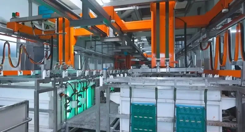
IPC Standards and Process Control
A factory’s quality system is your insurance. For ENIG, IPC‑4552 specifies the acceptable gold thickness, nickel thickness, and corrosion resistance parameters. At GREATPCB, we monitor our ENIG lines to the following controls:
- Gold thickness: 0.05–0.12 µm (IPC‑4552 Class 2/3)
- Nickel thickness: 3–6 µm with low phosphorus content for ductile solder joints
- Bath pH maintained at 4.5–4.7 with real‑time analyzers
- Continuous carbon filtration to remove nickel contaminants
For HASL, we ensure solder thickness uniformity is within IPC‑6012 requirements and that lead‑free alloys meet RoHS compliance. All boards undergo J‑STD‑003 solderability testing before shipping.
Frequently Asked Questions
What is the main difference between ENIG and HASL?
The main difference is surface flatness. ENIG is perfectly flat (<1 µm variation), making it ideal for fine‑pitch components. HASL has an uneven surface (5–25 µm variation) that can cause soldering problems with small parts.
Is HASL still used in PCB assembly?
Yes, HASL is widely used when boards contain through‑hole components or large SMT parts with pitch above 0.8 mm. It remains the most cost‑effective finish for many consumer and industrial designs.
Does ENIG have a longer shelf life than HASL?
Yes. ENIG maintains solderability for 12 months in sealed packaging. HASL typically performs well for 3–6 months before oxidation reduces wetting force.
What is black pad in ENIG and how can it be prevented?
Black pad is a brittle fracture at the nickel‑solder interface caused by phosphorus enrichment from poor plating control. Prevention includes keeping gold thickness between 0.05–0.12 µm, maintaining bath pH at 4.5–4.7, and using carbon filtration to limit nickel ion buildup.
Can I use HASL for BGA components?
Not if the BGA pitch is less than 0.8 mm. The uneven HASL surface can lead to open joints or bridging. ENIG is the safe choice for any ball‑grid array package to guarantee co‑planarity.
How much more does ENIG cost compared to HASL?
ENIG typically adds $0.08–0.15 per square inch, while lead‑free HASL adds $0.02–0.04 per square inch. The extra cost is often justified by higher assembly yield and longer storage life.
Is lead‑free HASL better than leaded HASL?
Lead‑free HASL meets RoHS requirements and has comparable solderability, but it requires a higher process temperature, which can increase thermal stress on the board. The surface flatness is similar to leaded HASL.
Which surface finish is better for high‑frequency PCBs?
ENIG is better. Its smooth surface reduces impedance discontinuities and skin‑effect losses in high‑speed signal traces. For RF designs above 5 GHz, ENIG is the recommended finish.
Conclusion: Make the Finish Fit the Mission
ENIG vs HASL is not about one being universally better—it is about matching the finish to your assembly density, budget, and reliability requirements. HASL gives you low cost and fast turns for simple boards. ENIG delivers the flatness, shelf life, and fine‑pitch performance that modern electronics demand.
At GREATPCB, we support both finishes with equal expertise. Our ENIG process is certified to IPC‑4552, with strict controls that keep gold thickness in the safe window and virtually eliminate black pad risks. For HASL, we can turn your 2‑layer prototype in as fast as 24 hours while maintaining consistent coating thickness. Our free DFM check will flag any design rules related to your chosen finish—whether it’s via‑in‑pad for HASL or gold wicking prevention for ENIG.
When you are ready to start your next PCB assembly project, contact GREATPCB for a quick quote. Our engineers will help you pick the perfect surface finish and deliver boards that assemble right the first time.

Related Posts
PCBA Prototype
July 10, 2026