
High Frequency
Assembly
High-Frequency PCB Manufacturing
High-frequency PCBs carry RF, microwave and other signals where the board itself forms part of the signal path. The laminate, copper, stackup and fabrication tolerances influence how that path performs.
GreatPCB provides high-frequency PCB manufacturing for projects that need their material and construction reviewed alongside the electrical requirements. From a prototype to a production order, the selected material, target impedance and inspection scope should be confirmed for the particular design.
Discuss your high-frequency PCB project
Review your material, stackup and impedance requirements with our team.
What Is a High-Frequency PCB?
A high-frequency PCB is designed for circuits in which the behavior of the signal path must be considered along with the components. Wireless modules, antenna feeds and microwave circuits are examples. High-speed digital designs can share some of the same material and signal-integrity concerns, although their requirements are not identical to those of an RF circuit.
There is no single frequency that makes the same material necessary for every design. An operating band, trace length, permitted loss and operating environment all influence the choice. A short connection and a long, phase-sensitive antenna feed can need different constructions even when they operate in the same frequency range.
Choosing Materials for High-Frequency PCBs
Material selection starts with the finished circuit, not a brand name alone. A laminate’s dielectric properties influence the transmission line, while its thickness, copper and bonding layers determine how that material is used in the stackup.
Dielectric Constant and Signal Propagation
Dielectric constant, or Dk, describes a material’s relative permittivity. Together with the geometry of a transmission line, it affects propagation and characteristic impedance. A stable, well-characterized value helps the designer choose dimensions that meet the required electrical behavior.
Lower Dk is not automatically the best choice for every circuit. The appropriate value depends on the design objective, including the required line dimensions and electrical length. Compare values measured with compatible methods and at relevant frequencies.
Dissipation Factor and Signal Loss
Dissipation factor, or Df, describes dielectric loss. A lower Df can reduce the dielectric contribution to signal attenuation, but it does not describe every source of loss in a finished board. Copper roughness, conductor geometry, plating and transitions also matter.
The length of the signal path matters too. Before choosing a laminate solely from its Df, consider the allowed loss across the complete path and the conditions under which it will operate.
Consider two hypothetical traces on the same laminate: one connects nearby RF components, while the other crosses the board to a connector. The longer path can contribute more conductor and dielectric loss. Its transitions and connector also belong in the link assessment. Neither the laminate data sheet nor circuit frequency alone describes the loss of the finished channel.
Thermal and Mechanical Requirements
Coefficient of thermal expansion (CTE) describes how a material changes dimension as temperature changes. Differences between materials and copper can contribute to stress during fabrication, assembly and operation. When a stackup combines different laminates, their thermal and mechanical behavior should be reviewed together with the bonding materials and manufacturing process.
| Property | Why it matters | What to check |
|---|---|---|
| Dk | Affects propagation and impedance with the line geometry | Test frequency, method, direction and material thickness |
| Df | Indicates dielectric contribution to loss | Test conditions and the circuit’s allowed loss |
| Copper profile | Influences conductor loss and the copper-to-dielectric interface | Foil type, finished construction and adhesion requirements |
| CTE | Helps assess expansion and stress across the construction | Temperature range, material direction and assembly conditions |
| Dielectric thickness | Influences trace geometry and the distance to a reference plane | Available laminate thickness and finished stackup tolerance |
An Example of Reading a Material Data Sheet
Rogers’ RO4000 data sheet gives the following material properties, measured in the Z direction. These are examples for understanding a data sheet; they are not a GreatPCB stock list or a promise that every construction is available.
| Laminate | Process Dk at 10 GHz and 23°C | Typical Df at 10 GHz and 23°C |
|---|---|---|
| RO4003C | 3.38 ± 0.05 | 0.0027 |
| RO4350B | 3.48 ± 0.05 | 0.0037 |
Rogers notes an exception for 4 mil RO4350B laminate: its listed process Dk is 3.33 ± 0.05. The data sheet also lists a separate design Dk measured by a different method. The distinction matters when comparing data sheets or entering a value in a design model. Source: Rogers RO4000 data sheet.
GreatPCB’s existing material pages discuss Rogers, Isola, Taconic and PTFE-based materials. Confirm the exact grade, thickness, copper and availability for your order. Our High-Frequency PCB Material Selection Guide explains how to compare material data and a complete board construction.

High-frequency PCB image.
Stackup and Controlled Impedance
The stackup establishes the relationship between the signal conductor and its reference plane. Trace width, finished copper thickness, dielectric thickness and material properties all influence characteristic impedance. Changing one part of the construction can therefore affect the line dimensions needed to meet the target.
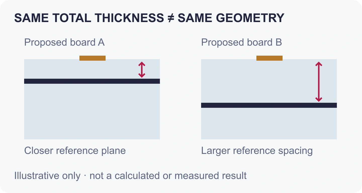
Reference-plane spacing is one factor that influences transmission-line geometry. Illustrative comparison, not a calculated result.
Microstrip and Stripline
A microstrip is an outer-layer trace referenced to a nearby plane. A stripline is an internal trace between reference planes. Each structure has different surroundings and manufacturing constraints; the appropriate choice depends on the circuit and the complete layer arrangement.
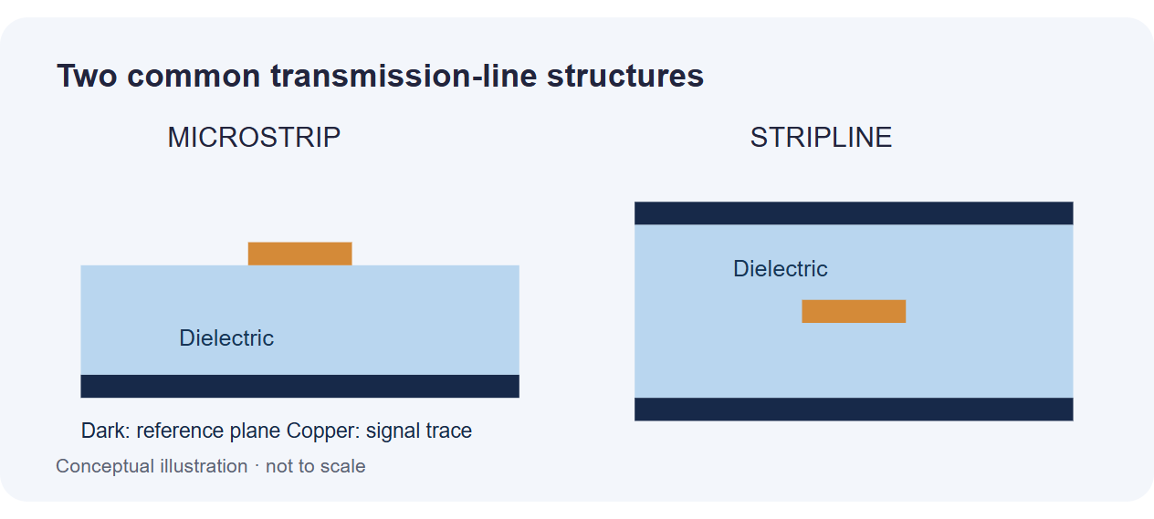
Microstrip and stripline position the signal trace differently relative to reference planes.
When a project calls for controlled impedance, the designer and fabricator should agree the target, tolerance, line geometry and proposed construction. Review the PCB stackup alongside the impedance requirements before production.
Copper, Return Paths and Transitions
Copper is more than a current-carrying layer. At higher frequencies, its surface profile can affect conductor loss, while trace geometry and the reference plane influence the electromagnetic field around the line. A smoother foil can help reduce roughness-related loss, but adhesion and processing requirements remain part of the material decision.
Changes in layer, connectors and vias introduce transitions into the signal path. Their effects depend on geometry and frequency; a board-level impedance target alone does not describe the behavior of every transition. Keep the signal path and its reference path in view when reviewing the design.
Manufacturing High-Frequency Boards
High-frequency laminates can have different drilling, lamination and surface-preparation requirements from a conventional epoxy-glass board. The exact process depends on the laminate family and the proposed construction, not simply on the label “high frequency.”
Lamination and Hybrid Stackups
A hybrid stackup combines material types in one board. It can place a selected RF material where the circuit needs it while using another material elsewhere. The materials and bonding layers must be compatible with the intended lamination process and operating conditions.
Before treating a substitution as equivalent, review its dielectric thickness, Dk and Df conditions, copper, thermal behavior and compatibility with the approved stackup. A change in one layer can require the impedance geometry to be recalculated.
The bonding layer is part of the electrical structure as well as the mechanical bond. If the field of a transmission line extends into that layer, its thickness and dielectric properties can influence the result. Material selection should therefore cover the core, bondply or prepreg, copper and finished geometry together.
Rogers’ RT/duroid 6000 fabrication guidance describes different adhesive systems and preparation for those specific laminates. It is an example of why processing must follow the material system; it is not a universal recipe or a statement of GreatPCB’s available process.
Drilling, Plating and Surface Finish
Hole formation and plating should be planned around the selected materials and the via structures in the design. For complex builds, registration and the integrity of plated holes are part of the manufacturing review.
Surface finish protects exposed copper and supports assembly, but its suitability also depends on the application and exposed RF structures. Select a finish with both assembly and electrical requirements in mind rather than assuming one finish is best for every board.
Inspection and Verification
Different tests answer different questions. A useful test plan states what is measured, where it is measured and the acceptance criteria.
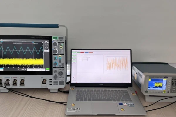
Electronic measurement equipment shown for illustration; the image does not establish a particular test or facility.
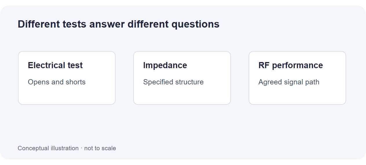
Electrical, impedance and RF measurements answer different questions.
| Method or requirement | What it addresses | What it does not establish on its own |
|---|---|---|
| Bare-board electrical test | Checks the relevant nets for opens and shorts | RF loss or the complete assembled circuit’s performance |
| Controlled-impedance verification | Checks specified test structures against an agreed impedance target and tolerance | Every transition or the insertion loss of the complete signal path |
| RF performance measurements | Can assess specified signal-path behavior over an agreed frequency range | Other reliability or assembly requirements unless separately defined |
Test coupons, methods, equipment and reports depend on the project and must be agreed before manufacture. Consult our PCB testing page for an overview of bare-board inspection; confirm the available impedance and RF measurement scope for the order.
From an Impedance Target to a Test Result
The specification should identify the relevant layers, line type, target impedance and tolerance. A test coupon is a representative structure manufactured with the board; its geometry and position should be appropriate for the intended verification. Time-domain reflectometry (TDR) can be used to examine impedance behavior along a test structure, subject to the agreed setup and interpretation.
The coupon is not the complete product channel. A result on a representative line does not automatically include the board’s connectors, every via transition or the assembled circuit. If insertion loss or return loss must be demonstrated over a specified band, define the structure, frequency range and measurement reference separately. Availability of equipment and reports is subject to project confirmation.
Example: Reviewing a Hybrid RF Board
Imagine a design with an RF trace on a low-loss outer laminate and digital circuitry in the remaining layers. The engineer specifies the intended material grade, copper and a controlled-impedance trace. During review, the fabricator checks the available thicknesses and bonding arrangement against the proposed construction. If a substitution changes the dielectric spacing, the trace geometry may need to be recalculated before the stackup is approved.
This is an illustrative scenario, not a GreatPCB production case. Its purpose is to show why material selection, stackup approval and test requirements should be discussed together.
Where High-Frequency PCBs Are Used
Wireless communication boards, antenna feeds and RF modules can have different requirements for impedance, loss and connector transitions. Radar and microwave circuits may also be sensitive to phase, material behavior and operating conditions.
An application name alone does not determine the stackup. A useful manufacturing discussion starts with the actual design, material requirements and acceptance criteria rather than assumptions based on the industry.
Frequently Asked Questions
Can FR-4 be used for a high-frequency PCB?
Sometimes. The decision depends on the actual laminate, operating frequency, path length, acceptable loss and other requirements. A low-loss material or hybrid construction may be appropriate when the complete circuit cannot meet its requirements with the proposed FR-4 construction.
Is a lower Dk always better?
No. Dk affects propagation and impedance together with line geometry. The preferred value depends on the circuit, desired dimensions and performance goals. Compare data at relevant conditions rather than choosing a material from Dk alone.
Does impedance testing prove the board meets every RF requirement?
No. Impedance verification checks the specified structure against an agreed target. A complete RF path may also have loss, phase or transition requirements that need a separate measurement and acceptance plan.
Can a different laminate be substituted?
A substitution should be reviewed before production. Compare the precise material grade, thickness, copper, dielectric properties and processing compatibility; then check whether the approved geometry and impedance requirements remain valid.
What affects the price and lead time?
Material grade and availability, board dimensions, layer count, hybrid construction, special processes and the required tests can all affect the quotation. The project team can review these factors against the actual design.
Get a High-Frequency PCB Quote
Discuss your material, stackup, impedance and inspection requirements with GreatPCB. We will review the project scope and provide a quotation based on the proposed construction.