
Drone PCB Assembly: Solving High-Density SMT Challenges
When Miniaturization Hits the Wall
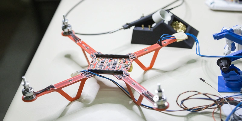
A drone developer brought us a failed flight controller last year. The board measured 28mm × 28mm — standard stack size. But they tried to pack a 6-layer HDI stackup, an STM32H7, dual IMUs, a barometer, and a 4A ESC power stage onto that footprint. The result? The drone flew fine for three test flights. On the fourth flight, it dropped from 80 meters.
We cross-sectioned the board. Three problems showed up immediately. First, the 0.25mm BGA pads under the IMU had insufficient solder volume. The joints looked fine on X-ray but cracked under vibration because the pad diameter left no room for proper fillet formation. Second, the power stage copper pour was only 1oz on inner layers. At 4A continuous, the board reached 130°C internally. The FR4 substrate started delaminating around the vias. Third, and most critical — the laser-drilled microvias in the 6-layer stack had an aspect ratio of 1.2:1. That's technically within IPC spec, but only if plating thickness is dead uniform. It wasn't. One via opened under thermal cycling.
This is what happens when high-density SMT design ignores real manufacturing limits. A drone PCB doesn't fail because the schematic is wrong. It fails because the physical board can't survive the environment it's designed for. The layout was electrically correct. The DFM was terrible. No pad fillet allowance. No thermal relief on inner power planes. No via redundancy on critical sensor nets. The board passed bench testing because bench testing doesn't vibrate at 400Hz.
When miniaturization hits the wall, adding more layers or shrinking trace widths stops being the answer. You need to design for the assembly process, not just the netlist.
What Drone PCB Assembly Actually Demands
When a PCB sits on a lab bench, the assembly requirements feel manageable. Standard FR-4, conventional SMT processes, normal reflow profiles — nothing unusual. But mount that same board on a quadcopter frame and everything changes.
The assembly house now deals with a board that must survive 10G maneuvers while weighing under 30 grams. Vibration isn't a test condition anymore. It's the operating environment. Every solder joint on that drone PCB assembly faces cyclic stress at frequencies that shake weaker connections apart within hours of flight time.
This creates real SMT challenges that don't show up in standard consumer electronics. Component selection shifts toward smaller packages — 0201 passives become common, not because designers want them, but because every milligram matters. These tiny parts demand tighter placement accuracy from pick-and-place machines. A 50-micron offset that passes inspection on a TV mainboard becomes a tombstoning risk on a drone controller packed with 0201s.
Thermal management gets complicated too. The airflow that cools a desktop circuit doesn't exist at 400 feet. Boards rely on copper pours and thermal vias alone. Reflow profiling for these designs means accounting for uneven copper distribution — some zones act as heat sinks during soldering, others heat up fast and risk component damage.
The assembly process itself requires more discipline. Mixed-technology boards with connectors, sensors, and RF sections on the same substrate mean multiple reflow passes or careful hand-soldering sequences. One rushed step and a $200 flight controller becomes scrap before it ever leaves the ground.
Component Placement Density and Its Discontents
In theory, packing components closer together shrinks board size and improves signal integrity by shortening traces. In practice, pushing high-density SMT to its limits creates a cascade of manufacturing problems that EDA software never warns you about.
Pad Spacing and the Reflow Shadow Zone
When a tall component sits next to a short passive, the larger body literally blocks hot air and infrared energy during reflow. The smaller part sits in a thermal shadow. Its solder paste may not reach liquidus at the same moment as the rest of the board. The result is inconsistent wetting across the assembly. I have seen 0201 capacitors on one side of an electrolytic can fail to reflow entirely while parts on the opposite side form perfect fillets. The fix is not always more soak time. Sometimes you must rotate the tall component 90 degrees relative to airflow direction or increase spacing beyond what the design rules permit by default.
Tombstoning and Thermal Mass Mismatch
Tombstoning happens when one end of a chip component lifts off the pad during reflow. The root cause is almost always a thermal or wetting imbalance. On high-density SMT boards, the problem gets worse because different copper densities on each pad create different heating rates. A pad connected to a large ground plane stays cooler. The opposite pad, tied to a thin signal trace, heats faster. The paste melts on one side first. Surface tension pulls the part vertical. This is not a theoretical edge case. It happens regularly on dense layouts where designers connect one pad directly to a pour and leave the other with a narrow thermal relief. The engineering decision is deliberate: balance pad connections thermally even when it means adding extra traces that serve no electrical purpose.
Thermal Management in Stacked Multilayer Boards
Managing heat in a multilayer PCB stackup isn’t about eliminating temperature—it’s about giving heat a predictable exit path before it warps your substrate or drifts your analog reference. The solutions sit at three levels: via structure, copper geometry, and laminate choice.
Thermal Via Arrays Under QFN and BGA Packages
A single thermal via under an exposed pad helps. An array of 0.3mm vias on a 0.8mm pitch works better. The real gain comes from plating thickness. Standard 1-mil barrel plating carries less heat than a 1.5-mil or 2-mil plated via. So when a design calls for 25μm plating, we sometimes bump it to 35μm just for the thermal vias under the hot components. Also, via fill matters. Conductive epoxy fill beats air-filled vias by roughly 8–10× in thermal conductivity. Non-conductive fill? Worse than air. It traps heat. We learned that on a power amplifier board where junction temperatures dropped 12°C just by switching from non-conductive to conductive plugging.
Copper Pours as Heat Spreaders
Inner-layer copper pours do double duty: current return and thermal spreading. A 2-oz plane pulls heat laterally much faster than a 1-oz plane. But here’s the constraint—etching fine traces on 2-oz copper is harder. So we often pour 2-oz on dedicated thermal layers and keep signal layers at 1-oz or 0.5-oz. The pour should extend well past the component footprint. A common mistake: stopping the pour at the package outline. Heat doesn’t stop there. Extend it 10–15mm outward when space allows.
Material Selection for High-Temperature Stacks
FR-4 works up to about 130°C Tg. Beyond that, the resin softens and Z-axis expansion delaminates via barrels. For multilayer PCB designs running hot—think LED arrays or automotive engine-compartment boards—we specify high-Tg FR-4 (170°C) or polyimide. The cost difference is real. High-Tg FR-4 adds maybe 15–20% to the substrate cost. Polyimide doubles it. But the alternative is field failure, which costs more. Also, ceramic-filled hydrocarbon laminates like Rogers 4000-series handle heat while maintaining stable dielectric constant. That matters when your thermal solution can’t compromise RF performance.
Mixed-Technology Assembly: 0201 Next to QFN
We saw this failure on a 12-layer automotive telematics board back in 2019. The design placed a 0201 decoupling capacitor 0.8mm from a 0.4mm-pitch QFN-48. The CAD looked clean. The stencil design did not.
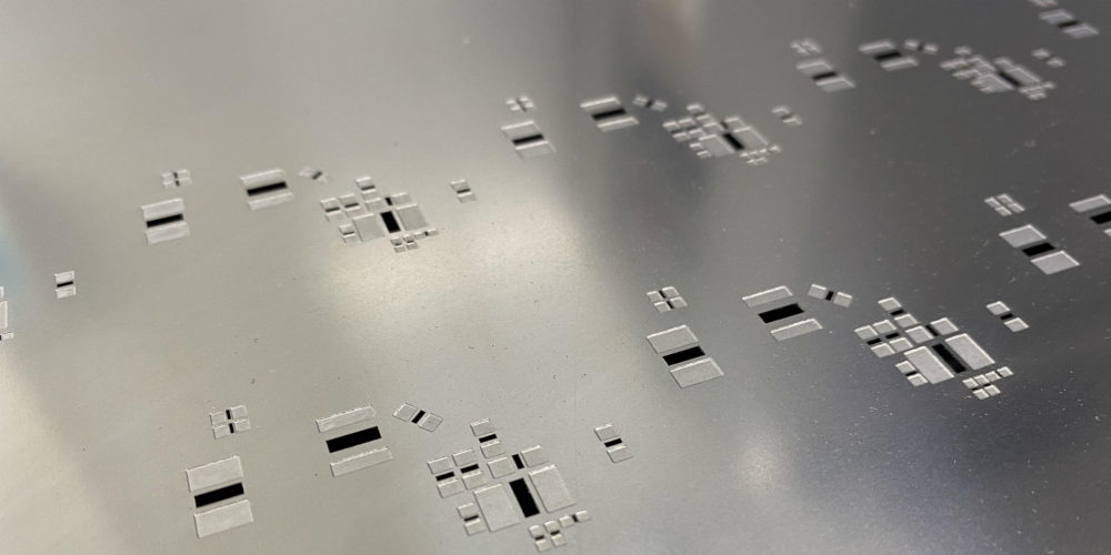
The core problem was solder paste volume mismatch across a single stencil. The QFN required a 0.1mm stencil thickness with 0.22mm square apertures to prevent bridging on the inner thermal pad and perimeter leads. But the 0201 pads, sized at 0.3mm × 0.35mm, needed at least 0.12mm thickness to achieve a reliable area ratio above 0.66. With the 0.1mm stencil, the 0201 aperture area ratio dropped to 0.58. Paste release became inconsistent.
On the first run, 23% of 0201 components showed insufficient solder after reflow. Some parts tombstoned. Others lifted entirely during ICT probing because the fillet height was below IPC-A-610 Class 2 minimums. The QFN side looked perfect — no bridges, full wetting on the exposed pad. But you cannot ship a board where one section passes and another fails.
Step Stencil as a Partial Fix
We tested a step stencil: 0.1mm base with a 0.12mm step-up pocket for the 0201 zone. This improved paste release for the small discretes without flooding the QFN pads. However, step stencils add cost and slow down cleaning cycles. The squeegee blade wears faster at the step transition. For a 500-unit NPI run this was acceptable. For 50,000-unit ramp, it was not.
The real manufacturing lesson was about pad geometry trade-offs. We reduced the 0201 pad width by 0.05mm — still within component manufacturer tolerance — which brought the area ratio back above 0.66 with a standard 0.1mm stencil. Paste deposition stabilized across the entire mixed-technology zone. Rework rates dropped below 0.5%.
This failure taught us that mixed-technology assembly is not just about placement accuracy. It starts with stencil aperture design and paste rheology. When your board combines fine-pitch QFNs with micro-passives, the DFM review must model paste release for every aperture size on the same stencil foil. If your contract manufacturer does not perform this analysis before cutting steel, expect rework.
For complex mixed-technology designs requiring tight process control, working with an assembly partner that offers in-house DFM review and stencil optimization becomes critical. At GreatPCB, our SMT Assembly Capability includes step stencil design support and paste deposit inspection for boards combining fine-pitch ICs with 0201 discretes, as listed in our SMT Capability table; smaller packages require separate engineering confirmation.
Via-in-Pad and Microvia Reliability Under Vibration
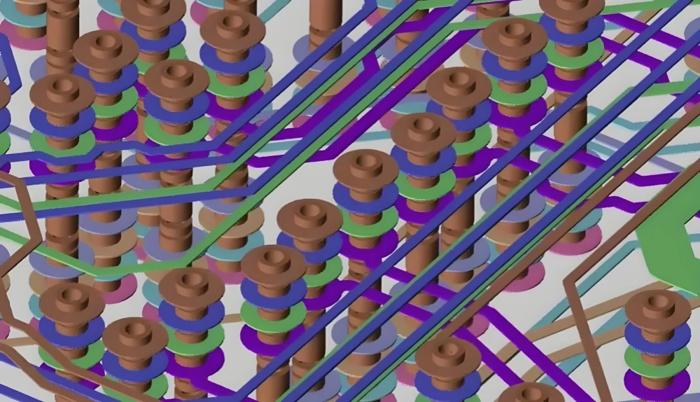
In vibration testing, we see a failure mode that textbook layouts miss entirely. A via-in-pad structure looks perfect in X-ray after assembly—complete fill, no voids, flat surface for the BGA ball. But after 200 thermal cycles and 6 hours of random vibration at 10G, cracks propagate through the copper at the pad-to-via interface. Not through the solder joint. Through the PCB itself.
Why the Fill Material Matters
The choice of via fill material directly controls stress distribution at this interface. Non-conductive epoxy fills work for thermal management but create a stiffness mismatch under vibration. The epoxy has a CTE of roughly 45 ppm/°C while the surrounding FR-4 is 14-16 ppm/°C in the Z-axis. When the board vibrates at resonance, this mismatch concentrates shear stress exactly where the via barrel meets the pad.
Conductive epoxy fills perform worse. The silver particles create micro-voids during curing. Under repeated vibration cycles, these voids act as crack initiation sites. I've seen cross-sections where cracks started at five separate void locations and connected into a single fracture plane within 500 cycles.
Copper-filled vias solve this problem but introduce a different one. The solid copper plug has near-zero compliance. During board flex, stress transfers entirely to the capture pad interface. IPC-6012 Class 3 requires that plated copper in the via barrel shows no cracks or separations after thermal stress testing. But vibration isn't thermal stress. The failure mechanism is high-cycle fatigue, not thermal expansion mismatch.
IPC-6012 Doesn't Cover This Gap
IPC-6012 defines acceptance criteria for microvia structures—target land diameter, wrap plating thickness, and void limits. It specifies thermal stress testing at 288°C for 10 seconds. This tests for plating integrity and material compatibility. It does not simulate the low-amplitude, high-frequency displacement that real-world vibration produces.
A via-in-pad that passes IPC-6012 Class 3 can still fail in field vibration within 18 months. The failure shows as intermittent opens. They only appear at specific resonant frequencies. Debugging this on an assembled board is nearly impossible because the crack closes when the board is static.
The Production Decision
For designs with both via-in-pad requirements and vibration exposure, copper-filled and planarized vias with a minimum wrap plating of 25μm outperform other options. The cost increase is 15-20% compared to epoxy fill. The alternative—field failures in automotive or aerospace applications—costs orders of magnitude more. We've learned to specify cross-section verification on first-article boards, specifically looking at the pad-to-via transition zone. IPC-6012 gives you a starting point. It doesn't guarantee vibration survival.
Signal Integrity at 6-Layer HDI Stackups
In a 6-layer HDI stackup, the move to laser-drilled microvias changes how we think about impedance control. You are no longer just calculating trace width and spacing against a reference plane. The cavity depth, the plating quality inside the microvia, and the dielectric thickness between layers 1–2 or 1–3 directly set the impedance. A 100µm microvia in a 60µm dielectric gives a different return path than a 200µm through-via in a standard board. I have seen designs where the differential pair was perfect on the routing layer but failed at the via transition because the antipad clearance was too tight for the thinner prepreg. The impedance dropped from 100Ω to 82Ω right at the launch. That is not a simulation error. That is a stackup decision that was not verified.
Crosstalk becomes harder to manage in dense routing because the dielectric spacing is so thin. On a standard board, you can push traces apart. On an HDI PCB, you often have parallel runs on layer 1 and layer 3, separated by only 50–70µm of prepreg. Broadside coupling happens even when traces are not directly stacked. The electric field fringe through the thin glass weave creates noise paths you do not see in a 2D field solver. Also, the via stub length in a 6-layer stackup matters more than people think. If you route from layer 1 to layer 4 using a buried via, the remaining stub on layer 6 acts as an antenna. I specify backdrilling on any via longer than 150µm when the signal rise time is below 50ps. Without it, the insertion loss plot shows a deep null at the resonant frequency. That null moves into the signal band on 25Gbps lanes.
The real design decision is choosing between a 1+N+1 or a 2+N+2 buildup. A 1+N+1 stackup keeps microvias on the outer layers only. A 2+N+2 allows stacked microvias but increases cost by 30–40% because of the extra lamination cycle. I choose 2+N+2 only when the BGA pitch forces me below 0.5mm. For rigid-flex PCB designs that combine HDI sections with flex layers, the impedance discontinuity at the rigid-to-flex transition needs separate verification. You cannot trust the same line width across both zones.
DFM Rules That Prevent Rework on Drone Boards
When a drone board comes back from assembly with bridging, tombstones, or open circuits, the root cause is rarely the soldering process itself. Most rework on dense UAV PCBs traces back to three geometry-level decisions made long before the stencil printer starts.

Pad Geometry That Matches Real Reflow Behavior
The standard IPC pad recommendations work for 0603 and larger parts. But on drone boards where 0201 passives sit next to tall power inductors, shadowing effects during reflow create uneven heating. The solution is not a universal pad shrink. Instead, pull back the pad width by 10–15% on the side facing the tall component while keeping the opposite pad standard. This asymmetric geometry gives both terminations a chance to reach liquidus simultaneously, preventing the standing component from pulling the part upright as it wets first.
For QFN packages with exposed thermal pads, segment the center pad into smaller squares separated by solder mask dams. A single large thermal pad acts as a solder sponge during reflow, starving the perimeter I/O pads and creating intermittent opens that only show up during vibration testing.
Fiducial Placement That Accounts for Panel Distortion
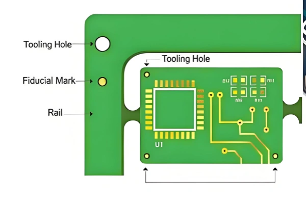
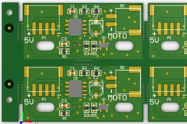
Three fiducials per board is standard advice. It is also wrong for panelized drone PCBs. During the first reflow pass, the panel warps non-uniformly because copper distribution varies across the array. Two global fiducials at opposite corners plus one local fiducial near fine-pitch BGA sites gives the pick-and-place machine enough data to interpolate true position. Without local fiducials, the machine assumes linear distortion, but the actual warpage is parabolic across the panel span.
Panelization Rules That Survive Depanelization
V-score works for rectangular boards with no edge-mounted connectors. Drone boards rarely meet that condition. Most have castellated edges for stacking or side-mounted U.FL connectors that cannot tolerate the bending stress of v-score breakout. Route-and-tab panelization with mouse-bite breakaways keeps edge geometry clean, but tab placement matters. Position tabs at least 8mm away from any MLCC footprint larger than 0805. The flexing during depaneling travels through the laminate and cracks capacitors that pass electrical test but fail after thermal cycling.
For rigid-flex PCB designs that combine rigid sections with flex layers, the panelization must also account for the different expansion rates during assembly. A rigid-only panel frame with the flex areas left unsupported prevents the flex material from sagging into the reflow oven mesh.
Frequently Asked Questions
Thermal Mismatch Between Rigid and Flex Layers
In production, we see this failure most often when boards come out of the reflow oven. The rigid FR-4 section and the polyimide flex layer expand at different rates. At 250°C peak reflow temperature, the difference is small but measurable. When the board cools, the materials contract at different speeds. This puts stress on the junction where rigid meets flex.
The failure doesn’t always show immediately. Sometimes the trace cracks are microscopic. They pass electrical test at the factory. But after a few thermal cycles in the field, the crack propagates and the drone loses a motor signal mid-flight.
The fix is not in the materials. You can’t change the expansion coefficients of FR-4 and polyimide. The fix is in the stack-up design. Adding a strain relief fillet at the rigid-flex transition point helps distribute the stress. Also, routing traces perpendicular to the bend line rather than parallel reduces the risk of copper fracture.
Minimum Bend Radius Violations
I’ve reviewed too many designs where the mechanical engineer specifies a bend that the flex material cannot survive. A 2-layer flex with 1oz copper has a minimum bend radius of about 6x the total thickness. For a 0.2mm flex, that’s 1.2mm radius. But designers often push for 0.5mm or tighter because the drone body is compact.
The failure mode is predictable. The copper work-hardens at the bend point. After repeated folding during assembly or vibration during flight, the trace resistance increases. Eventually it goes open. We catch this during design review when the bend radius calculation doesn’t match the mechanical enclosure requirements.
Stiffener Placement and Component Keep-Out
This is a layout issue that shows up during assembly. Components placed too close to the rigid-flex boundary experience higher stress during depaneling. The router bit or laser cutting process creates micro-vibrations. If a 0402 capacitor sits 0.5mm from the edge, the solder joint cracks before the board leaves the factory.
The rule we enforce is a 2mm component keep-out zone from any flex transition edge. For stiffeners, the adhesive squeeze-out during lamination can contaminate nearby pads. We’ve seen solderability issues on ENIG surfaces where adhesive residue wasn’t fully cleaned before plating.
Via Placement in Flex Sections
Vias in the dynamic flex area are a reliability risk. The copper plating inside the via barrel cracks under repeated bending. This is worse with smaller vias. A 0.2mm via in a flex section that bends 10,000 times during the drone’s lifetime will fail statistically sooner than a 0.3mm via.
The better approach is to keep all vias in the rigid sections only. If you must have vias in the flex area, use teardrop reinforcements and limit them to static bend regions only. For dynamic flex zones, no vias at all.
For flex PCB assembly projects, we always check the via map against the mechanical bend profile before approving the design. This is a standard DFM checkpoint that catches most field failures before they happen.
Engineering Support for Your Next Drone Build
Before you release a drone design to fabrication, send the full stackup and board outline to a manufacturer that understands mechanical stress. I've seen rigid-flex builds fail because the via array crossed the neutral bend axis — something a standard electrical DRC never flags. A proper DFM review catches this. It checks copper balance, solder mask clearance near castellated edges, and component placement relative to mounting points. For prototype PCB assembly, the review should also verify BOM completeness against the pick-and-place file. Missing a single polarity mark on a connector footprint can delay a flight test by two weeks. If you need a manufacturing partner who reads your design like an engineer — not just a CAM operator — request a DFM review or a prototype PCB assembly quote. Our team supports builds from 5-unit prototypes to full production runs across our prototype PCB assembly line and dedicated SMT production line.