
IPC Class 3 PCB Manufacturing & Assembly
When failure is not an option, trust GreatPCB's IPC Class 3 certified manufacturing. We deliver high-reliability printed circuit boards for aerospace, medical, military, and mission-critical applications — backed by rigorous testing and 100% inspection.
What Is IPC Class 3?
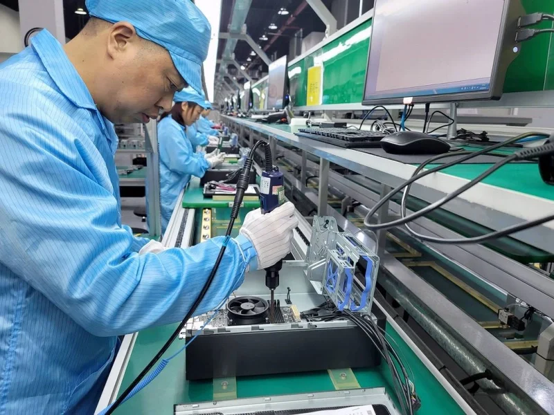
IPC Class 3 represents the highest level of reliability in printed circuit board manufacturing, as defined by the IPC-6012 standard. Unlike Class 1 (general electronics) or Class 2 (dedicated service), Class 3 boards are engineered for applications where downtime is not an option and failure could endanger human lives.
At GreatPCB, we manufacture IPC Class 3 PCBs with stringent controls over plating thickness, annular ring integrity, dielectric spacing, and solderability — ensuring every board meets or exceeds the rigorous demands of aerospace, medical, and defense industries.
Core IPC Class 3 Capabilities
From advanced multilayer designs to ultra-fine traces, our IPC Class 3 manufacturing line is equipped to handle your most challenging requirements with precision and repeatability.
Multilayer PCBs Up to 40+ Layers
We manufacture complex multilayer boards with precise layer registration, ideal for high-density interconnect (HDI) and advanced aerospace systems.
High-Frequency & RF Materials
Expertise in Rogers, Taconic, Isola, and PTFE-based laminates for RF/microwave applications requiring tight impedance control.
Blind & Buried Via Technology
Advanced via-in-pad, stacked microvias, and staggered via structures to maximize routing density in compact form factors.
Comprehensive Surface Finishes
ENIG, ENEPIG, HASL (lead-free), Immersion Silver, Immersion Tin, and Hard Gold — all applied under Class 3 process controls.
Fine-Pitch & BGA Support
Trace width/spacing down to 3/3 mil with precise solder mask alignment for fine-pitch BGAs and QFNs.
Strict Quality Assurance
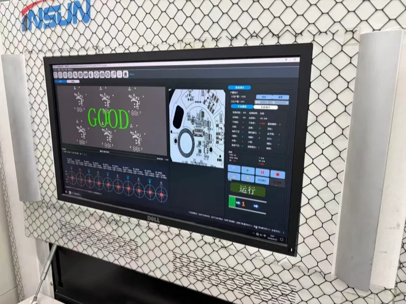
Every Class 3 board undergoes AOI, microsection analysis, solderability testing, and 100% electrical test before shipment.
IPC Class 3 Specifications
Our manufacturing capabilities align with the strictest IPC-6012 Class 3 requirements. Here's how we measure up.
| Parameter | IPC Class 3 Requirement | GreatPCB Standard |
|---|---|---|
| Max Layer Count | As per design | Up to 40+ Layers |
| Min Trace Width / Spacing | Per design rules | 3 / 3 mil |
| Plated Through-Hole Copper | ≥25μm (1 mil) | ≥25μm, verified via microsection |
| Minimum Annular Ring | ≥50μm (2 mil) | ≥50μm, with 100% AOI verification |
| Dielectric Spacing | ≥90μm | ≥100μm (exceeds standard) |
| Solder Mask Registration | ≤50μm misregistration | ≤35μm (tight tolerance) |
| Surface Finish Options | Multiple | ENIG, ENEPIG, HASL (LF), Imm Ag, Imm Sn, Hard Gold |
| Impedance Control | ±10% | ±5% (precision option available) |
| Electrical Testing | 100% required | 100% flying probe + bed-of-nails where applicable |
Advanced Manufacturing Equipment
GreatPCB's Class 3 production floor is equipped with state-of-the-art machinery, ensuring precision, repeatability, and scalability for your most demanding projects.
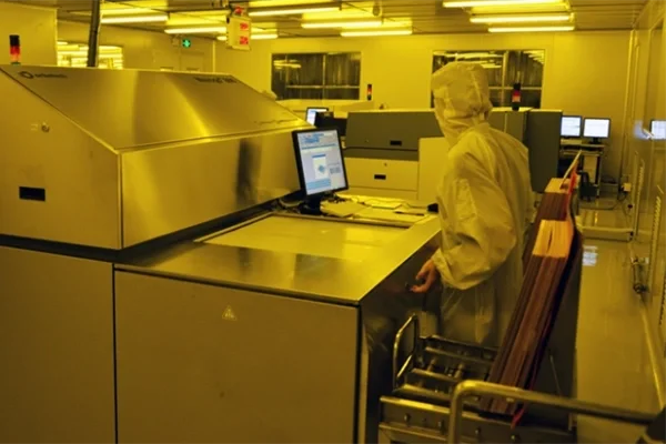
Laser Direct Imaging (LDI)
High-precision patterning for ultra-fine traces and exact layer registration.
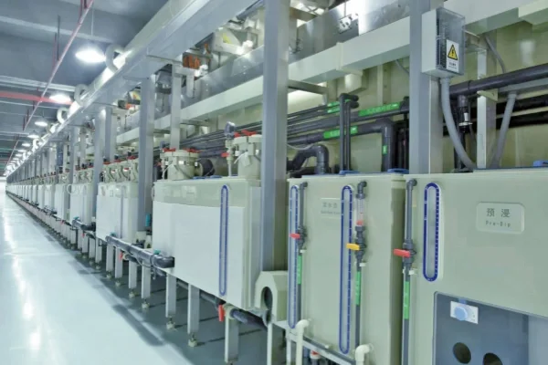
Vertical Continuous Plating
Uniform copper deposition ensuring ≥25μm hole wall thickness for Class 3 compliance.
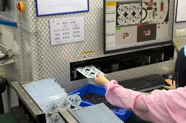
Automated Optical Inspection (AOI)
100% board scanning for trace defects, shorts, opens, and solder mask alignment.
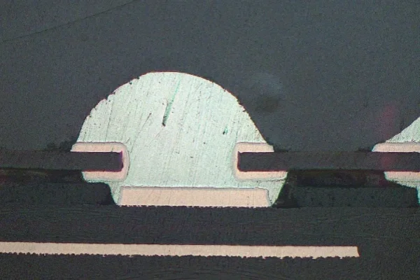
Microsection Analysis Lab
Cross-sectional verification of plating thickness and via integrity on every lot.
 />
/>Flying Probe Electrical Test
High-speed continuity and isolation testing for complex, high-layer-count boards.
 />
/>TDR Impedance Measurement
Verification of controlled impedance traces within ±5% for RF and high-speed designs.
Why Engineers Trust GreatPCB for Class 3
Delivering high-reliability PCBs isn't just about meeting a standard — it's about consistency, transparency, and a commitment to excellence at every step.
Years of Experience
Serving demanding industries with high-reliability PCB solutions since our founding.
First-Pass Yield
Industry-leading yield rates on Class 3 boards, verified by rigorous in-process controls.
Layer Capability
From simple 2-layer to complex 40+ layer HDI boards — all under one roof.
Engineering Support
Dedicated DFM review and technical consultation throughout your project lifecycle.
Applications of IPC Class 3 PCBs
IPC Class 3 boards are mission-critical. Here are the industries that rely on our high-reliability manufacturing.
Rigorous Inspection & Testing
Every IPC Class 3 board leaving our facility undergoes a comprehensive battery of tests to guarantee reliability in the field.
- Automated Optical Inspection (AOI) — 100% of boards scanned for surface defects, solder mask alignment, and trace integrity.
- Microsection Analysis — Cross-sectional verification of plating thickness, via structure, and dielectric integrity on every lot.
- Impedance Testing — TDR-based impedance verification for controlled-impedance designs, ensuring ±5% accuracy.
- 100% Electrical Test — Flying probe and bed-of-nails testing to verify continuity and isolation on every single board.
- Solderability Testing — Per IPC-J-STD-003 to ensure reliable assembly and long-term joint integrity.
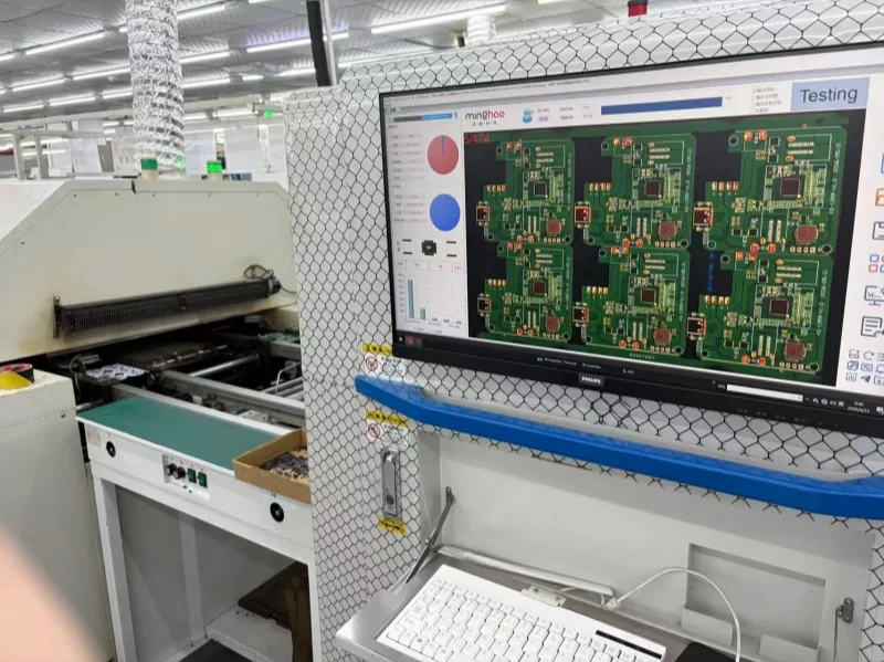
Explore More About GreatPCB
Learn more about our manufacturing infrastructure, quality commitments, testing capabilities, and answers to common questions.
Our Factory
Tour our advanced manufacturing facility and see the equipment behind our Class 3 capability.
View FactoryPCB & PCBA Packaging
A systematic approach ensures every order receives consistent, reliable protection — from the production floor to your loading dock.
View PackagingTesting & Inspection
Dive deeper into our inspection protocols, from AOI to microsection analysis and electrical test.
Explore TestingFAQ
Find quick answers to common questions about IPC Class 3, lead times, and ordering process.
View FAQ