
QFN Soldering Problems: Causes, Inspection and How to Prevent Defects
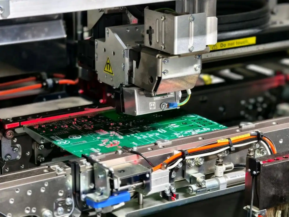
A QFN component can look correctly placed and still cause trouble after reflow. One board may fail to power up, another may have a short between adjacent nets, and a third may pass an electrical check while the condition of its center pad remains unknown.
The difficulty is that much of a QFN’s solder connection is hidden beneath the package. When a problem appears, the cause may be in the PCB footprint, solder paste deposit, component alignment, reflow process or inspection plan. Looking at the part from above rarely identifies the cause by itself.
This guide explains the most common QFN soldering problems, what to check before and after assembly, and which details to discuss with your PCB assembly partner.
Why Is QFN Soldering Different?
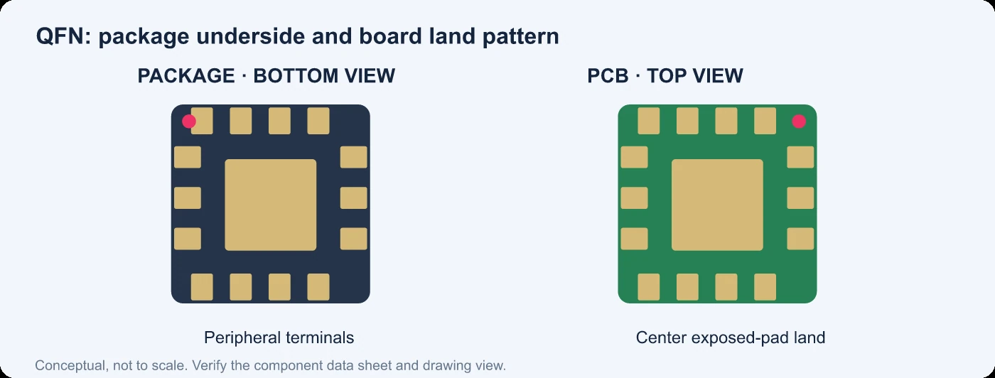
QFN terminal and PCB pad arrangement. Illustration is conceptual and not to scale.
QFN stands for quad flat no-lead. Instead of protruding gull-wing leads, the package has metal terminals around the underside of its four edges. Many QFNs also have an exposed pad in the center of the underside.
The peripheral terminals connect the device to the circuit. Depending on the component, the center pad may provide a thermal path, an electrical connection or both. Its required connection should be taken from the exact component data sheet; it should not automatically be treated as ground.
The solder joints are mostly underneath the package
After assembly, the component body covers much of the joint area. Magnification can help an inspector see alignment and accessible edges, but it cannot show the entire center-pad connection. Electrical tests can reveal certain opens or shorts, while X-ray can provide a view of hidden solder features.
These checks answer different questions. A board that powers on has passed one useful check; it has not necessarily proved that every QFN joint meets the project’s inspection or reliability requirements.
Small changes can affect the result
Fine-pitch peripheral pads need controlled paste deposits and accurate placement. The larger center pad presents a different challenge: its paste deposit must form the intended connection without preventing the package from settling appropriately onto the outer pads.
Footprint dimensions, stencil openings, printed paste, thermal vias and reflow conditions work together. Changing one of them may affect the result of the others.
Common QFN Soldering Defects
| Problem | What you may notice | Start by checking |
|---|---|---|
| Solder bridge | A short between adjacent pins or between a pin and the exposed-pad net | Paste deposit, stencil alignment, placement and the reflowed joint |
| Open joint | An expected connection is missing or a function does not operate | Footprint, pad numbering, paste coverage, alignment and thermal profile |
| Tilted or shifted component | Package position or visible joints appear uneven | Paste distribution, component placement and board support |
| Insufficient center-pad connection | Thermal or electrical behavior does not meet the design requirement | Pad and via design, paste pattern, X-ray and the agreed test method |
| Voiding | X-ray shows voids within the soldered region | Solder materials, via treatment, reflow and the applicable acceptance criteria |
The same symptom can have more than one cause. A short may result from a bridge, a footprint error or a design connection that was intended; check the schematic and netlist before treating every low-resistance reading as a soldering defect.
Bridges and shorts
Fine-pitch pads leave limited room for a solder deposit to spread. Excessive or misaligned paste, smearing during printing, component movement and an unsuitable stencil aperture can contribute to solder bridges.
Begin with the affected pads and compare the PCB, component data sheet and stencil design. If inspection images or paste-print records are available, compare them with a known-good board before changing the process.
Open or intermittent connections
An open can occur when insufficient solder reaches a pad, a terminal is misaligned or the joint does not form as intended during reflow. But a failed signal can also come from an incorrect footprint, an unconnected PCB net, a damaged component or the test setup.
Check accessible electrical paths and assembly records first. Where the joint is hidden, an appropriate X-ray or other agreed inspection method can add information that a top view cannot provide.
Voids under the center pad
A void is an area without solder within a soldered joint. Voids can be visible on an X-ray image, but their effect and acceptance depend on the package, the function of the exposed pad, the measurement method and the agreed standard or product requirement.
Do not assume that every visible void is a failure—or that a single percentage is suitable for every package. Establish how the void area will be measured and what criteria apply before production.
Check the Footprint Against the Actual QFN
Before changing solder paste or oven settings, confirm that the PCB was designed for the component that will actually be assembled.
Match the complete part number and package drawing
Compare the manufacturer’s package drawing with the PCB land pattern. Check the package body, terminal count and pitch, peripheral land dimensions and center-pad arrangement. Similar package names can cover different sizes or terminal layouts.
Pay particular attention to the drawing view. A bottom view of the package and a top view of the PCB may appear mirrored. Map the terminals by number, not by visual resemblance alone.
Check Pin 1 and placement orientation
Confirm that the component marking, PCB land pattern, assembly drawing and schematic agree on Pin 1. Then check how the placement system interprets the component’s zero rotation and origin.
A placement file coordinate describes a reference point; it does not by itself tell an operator where Pin 1 is located. Our pick and place file guide explains origins, sides and rotations in more detail.
How Stencil Design Affects QFN Soldering
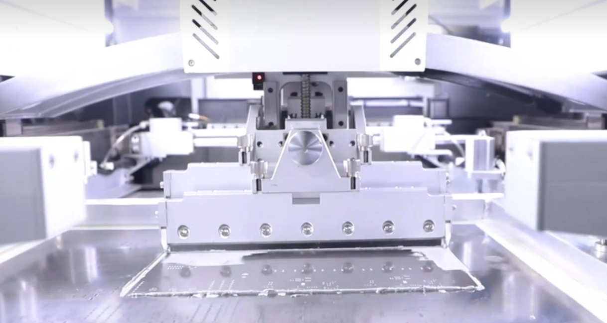
Solder paste printing is one step in surface-mount assembly.
The stencil determines where solder paste is printed and influences how much paste can be deposited. For a QFN, the outer terminals and the large exposed pad should be considered together.
Peripheral pads: control the deposit
Small openings must release paste consistently onto the PCB. Aperture shape and size, foil thickness, paste characteristics and printing conditions all matter. A printed deposit that is offset, smeared or incomplete is a reason to investigate before components are placed.
Reducing an aperture is not automatically the answer to every bridge. A change that limits excess paste must still leave enough solder to form the intended joint. Review the whole board: a stencil that suits one QFN must also work with the other components on the same side.
Center pad: why use multiple openings?
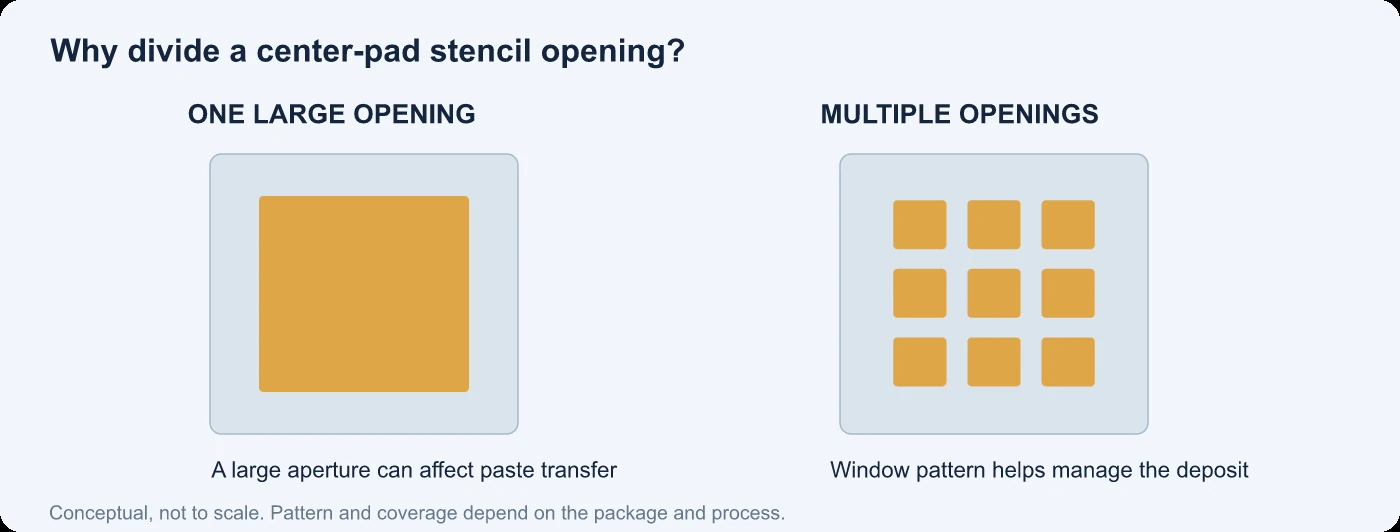
The aperture pattern and paste deposit must be assessed with the specific assembly process.
A large single opening can deposit more paste than intended. Too much paste under the center can affect how the package settles and how the surrounding joints form.
One common approach is to divide the exposed-pad aperture into several smaller openings. This distributes the deposit across the pad and gives the process team another way to manage solder volume.
For example, Analog Devices’ guidance for its specified standard wire-bonded QFN packages recommends multiple openings and describes 50–80% paste coverage for the exposed pad. This is a manufacturer guidance range for the packages and process context covered by that document, not a universal acceptance limit or a GreatPCB equipment specification. The selected component data sheet and assembly process remain the starting point.
Windowing can also help with print consistency. A squeegee can dip into a large stencil opening and remove some paste as it passes, leaving less paste than expected in the middle. Smaller openings support the blade across the pad area, although they must still release paste reliably. The Freescale PQFN assembly note discusses this effect for its power-QFN package family.
A published fine-pitch assembly example
One Chinese-language assembly study examined a 2 × 2 mm QFN with 0.4 mm terminal pitch on FR-4. The reported process used SAC305 paste and a 0.10 mm laser-cut stencil. The authors inspected 120 assembled components and reported that 113 had an exposed-pad void area below 10%. They also reported electrical continuity checks and environmental tests on the assembled parts. Study: Fine-pitch QFN soldering process design.
These are the authors’ results for that specific component and process—not a GreatPCB production result or a universal acceptance threshold. The report combines several design and process choices, so the result alone does not establish how much improvement came from any one stencil feature.
Inspect the actual print
The CAD paste layer is a design input, while the printed deposit is the result that enters placement and reflow. If solder paste inspection is included in the build, review the deposit’s position, completeness and consistency against the agreed process criteria.
What About Thermal Vias Under a QFN?
Thermal vias can help conduct heat from an exposed pad into other copper layers. Their size, location and treatment should be reviewed with the package requirements and the board manufacturer.
An open via in a soldered pad can also draw molten solder away from the intended joint. Depending on the design and fabrication approach, engineers may consider options such as tenting, plugging, filling or capping. Each changes the construction and may affect cost and manufacturability.
The question is not simply whether a via is visible. The drawing should identify the required treatment, and the stencil and assembly plan should account for the actual board construction. See our via-in-pad guide for the differences between these treatments.
Before release, look at the via pattern and the paste openings together. A via beneath a paste deposit may affect where solder travels during reflow, while a change to via treatment can alter the finished pad surface. Ask the board fabricator and assembler to review the chosen construction, paste pattern and inspection plan as one package.
Reflow or Hand Soldering: Which Method Fits the Job?
| Method | Common use | Main consideration |
|---|---|---|
| Stencil printing and reflow | Prototypes and production assemblies | Control paste printing, placement and the board’s reflow profile together |
| Hot-air rework | Removing and replacing an individual component | Manage heat, protect nearby parts and inspect the repaired site |
| Soldering iron | Accessible external joints or limited touch-up | The center pad and hidden terminals may not be reachable or verifiable |
For a board with many surface-mount components, stencil printing and reflow provide a repeatable assembly route. For a single prototype or repair, an engineer may use local heating, provided the component and board can be heated and inspected appropriately.
The heater setting is not the joint temperature
A hot-air station or hot plate display describes the equipment setting, not necessarily the temperature at every solder joint. Board thickness, copper planes, nearby components and airflow affect how heat reaches the QFN.
Use the solder paste supplier’s profile and the component’s temperature and moisture-handling requirements when establishing the process. A profile suitable for one board should not automatically be copied to another.
For troubleshooting, compare temperature measurements at representative locations on the board with the paste and component requirements. A heavy copper region may heat differently from a small exposed area. Also review the component’s moisture-sensitivity labeling and handling history before rework; use the applicable manufacturer’s instructions rather than an assumed baking time.
How to Inspect QFN Solder Joints
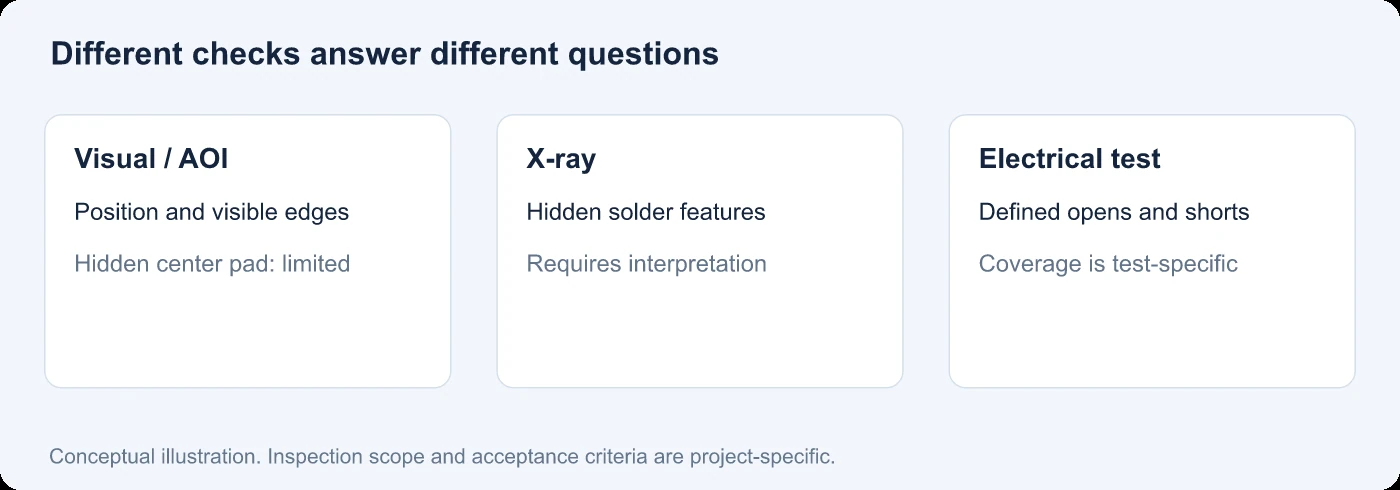
Inspection methods provide different types of evidence.

X-ray equipment can support inspection of hidden solder features.
| Method | What it can help assess | Important limitation |
|---|---|---|
| Visual inspection or microscope | Orientation, alignment, visible edges and some external bridges | The body obscures the center pad and much of the bottom terminals |
| AOI | Visible position, orientation and accessible solder features | Coverage depends on package geometry and what the camera can see |
| X-ray | Hidden solder regions, some bridges and void features | Images must be interpreted against an agreed method and criteria |
| Electrical or functional test | Specified opens, shorts and operating functions | A pass does not by itself prove every joint’s long-term reliability |
Can AOI inspect every QFN joint?
No. Some QFN variants have side-wettable flanks, designed to form an externally visible solder feature that can improve optical inspection. Other variants do not provide the same visible surface. Analog Devices describes several side-wettable package designs.
Even with a side-wettable device, inspection coverage depends on the package, camera access and acceptance plan. Optical inspection does not reveal the full condition of a hidden center pad.
Does every QFN need X-ray?
Not necessarily. Consider the package, circuit importance, production volume, access to other tests and required acceptance evidence. For a critical or difficult-to-observe connection, X-ray may be valuable; the scope and sampling should be agreed for the project.
Our PCB assembly testing guide compares inspection and electrical test methods in more detail.
What to Send Your Assembly Partner Before a QFN Build
A clear build package helps the assembler review the part and its soldering requirements before the first board is assembled:
- BOM: full manufacturer part number, package and approved alternatives.
- PCB manufacturing files: copper, solder mask and paste data, with board revision identified.
- Assembly drawing and placement file: reference designators, board side, component orientation and Pin 1 information.
- Component documentation: the applicable package drawing and any special exposed-pad or thermal requirements.
- Via treatment: identify vias in or near the exposed pad and specify the intended fabrication treatment.
- Inspection and testing: state whether visual inspection, X-ray, electrical checks or functional testing are required, along with the agreed acceptance criteria.
If a QFN is particularly important to the product, identify it in the build notes. A focused review of that component’s footprint, paste pattern and inspection requirements can be more useful than a general instruction to “check all solder joints.”
Frequently Asked Questions
Can QFN components be soldered without a stencil?
Yes, individual parts may be assembled or reworked without a full-board stencil using suitable equipment and controlled paste application. The practical approach depends on pitch, package geometry, available tools and how the joints will be inspected. A stencil is helpful when consistent paste deposits are needed across multiple boards.
Why is my QFN shorted after reflow?
Possible causes include a solder bridge, smeared or excessive paste, misalignment, a footprint or pin-mapping error, or an intended connection between the exposed pad and a peripheral pin. Compare the schematic and netlist first, then inspect the relevant assembly features.
Can a QFN be reworked?
Yes. A QFN can be removed and replaced using an appropriate rework process. The team must control the heat applied to the device and board, prepare the pads, place the replacement accurately and inspect the result. Repeated heating or mechanical force can damage pads and nearby components.
Does a center-pad void mean the assembly has failed?
Not automatically. The acceptance decision depends on the applicable product requirement, package guidance, inspection method and agreed criteria. A void image alone does not describe the device’s complete electrical, thermal or reliability performance.
Is the exposed pad always connected to ground?
No. Many designs connect an exposed pad to ground or a thermal plane, but its electrical function is device-specific. Follow the exact component data sheet and circuit design.
Plan the QFN Assembly Before Production
Reliable QFN assembly starts before the board enters the reflow oven. Matching the part to the footprint, reviewing the stencil and thermal vias, controlling paste deposits and selecting the right inspection methods all contribute to a better build plan.
If your board includes QFN or other fine-pitch components, share the BOM, PCB files, assembly drawings and test requirements with GreatPCB. We can review the assembly scope alongside your project requirements.
Table of Contents
- Why Is QFN Soldering Different?
- Common QFN Soldering Defects
- Check the Footprint Against the Actual QFN
- How Stencil Design Affects QFN Soldering
- What About Thermal Vias Under a QFN?
- Reflow or Hand Soldering: Which Method Fits the Job?
- How to Inspect QFN Solder Joints
- What to Send Your Assembly Partner Before a QFN Build
- Frequently Asked Questions
- Plan the QFN Assembly Before Production
Tags
Related Posts

PCBA Prototype
October 30, 2026
PCBA Prototype
October 30, 2026
PCBA Prototype
October 29, 2026