
PCB Programming Pads: How to Design for Repeatable Pogo Pin Contact

If a board programs when you hold the probes by hand but fails in a fixture, check two things with the PCB fully seated. Can each probe still land on exposed copper at the worst expected sideways shift? Does each probe compress enough at the clamp stop, including where the board can flex? Once both checks pass, unload and reload assembled boards to verify the electrical connection, programming, and firmware readback or checksum separately.
The example below follows the same board throughout. It uses flat programming pads and an edge-locating nest because there are components on the opposite side where new tooling holes might otherwise go. All example dimensions and compression limits are teaching values.
Define What the Fixture Must Connect
Map Programming Signals, Reference Voltage, and Power
Start with the target device’s programming requirements and the pinout of the selected programmer. Map each required net to the PCB pad, fixture probe, and programmer connector before sending coordinates to the fixture builder. Draw the power path separately so the operator knows what powers the board and when to apply it.
| Connection role | SWD example | What to confirm before laying out pads |
|---|---|---|
| Programming signals | SWDIO and SWCLK | Match the device pinout to the programmer. Check whether the workflow needs reset or any additional signals. |
| Ground | Programmer and target ground | Document the ground connection and verify it at the fixture. |
| Target voltage reference | VTG on Atmel-ICE | Connect according to the programmer’s reference-voltage requirements. |
| Board power | A separate supply or the board’s normal power input | Specify the voltage, source, and power-up order. Atmel-ICE’s VTG senses the target voltage, so the target needs its own power path. |
For the differences between programming loose devices and programming an assembled board, see GreatPCB’s IC programming overview.
Pick an Accessible Contact Area on the Assembled Board
Review the assembled PCB from both sides. Check clearance for the probe head, clamp, and supports through the full loading motion. Include connector overhangs, tall parts, and any areas the tooling would press on. Check the footprint of the probe assembly as well as the diameter of its tip.
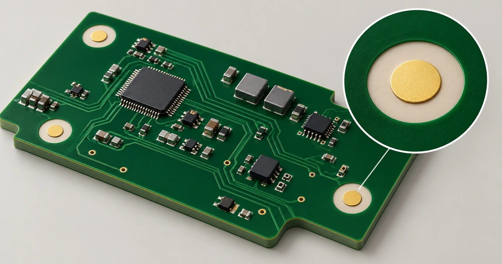
On the example board, the pads face down toward the probes. A nest locates the board against two perpendicular edges and leaves space around the populated areas. If those edges have irregular tab remnants or connector overhangs, try an existing tooling feature or another stable edge. Confirm that the chosen feature is defined and toleranced on the fabrication drawing. For any via used as a contact target, check whether the finished board exposes usable metal and whether the tip geometry suits the opening.
Check Where the Probes Land
Reference the Pads and Fixture to the Same Datum
Identify the exact edges or tooling features that seat in the nest. Give the fixture builder pad coordinates relative to those features, with units, board revision, the contact side and a view-orientation note. Have the builder compare the fixture’s pin-one position against the assembled board before machining the probe plate. Bottom-side plots and fixture views can be mirrored relative to each other.
A board can both translate in its nest and rotate around a locating feature. For the same angle, a pad farther from that feature moves more. On the example board, a 0.35° rotation shifts a pad 20 mm from the pivot by approximately 0.122 mm. Check the most exposed positions in the pad group, even when the pads nearer the locator look centered.
Compare the Contact Window With the Landing Error
For a round flat tip, one conservative screening test is to keep its entire effective contact footprint within the usable exposed copper. The allowable center offset is half the difference between the usable exposed diameter and the effective tip footprint. Use the opening where it actually overlaps copper after registration tolerances. Use the probe supplier’s tip geometry to establish the footprint or have the fixture builder characterize it.
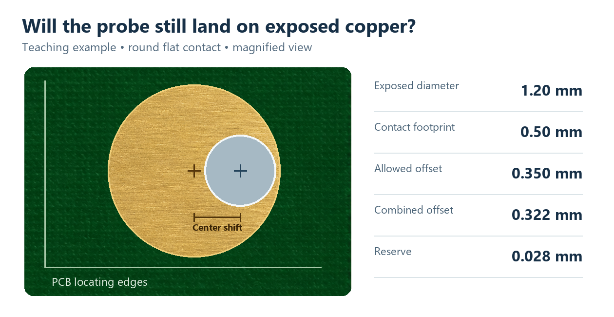
Figure 1. The silver circle represents the probe footprint. In the modeled worst direction, the footprint stays inside the exposed copper with 0.028 mm remaining.
| Item | Example | How it enters the check |
|---|---|---|
| Usable exposed diameter | 1.20 mm | Assumes copper covers the guaranteed usable area of the opening. |
| Effective flat-tip footprint | 0.50 mm | Uses the assumed maximum circle of contact. |
| Allowable center offset | 0.350 mm | (1.20 − 0.50) ÷ 2 |
| Translation, probe placement, and rotation | 0.140 + 0.060 + 0.122 mm | Added in the same direction as a conservative bound. |
| Remaining modeled margin | 0.028 mm | 0.350 − 0.322 mm |
This example clears the geometric screen with little room for uncounted variation. If copper or mask registration is missing from the opening estimate, include it before calling the layout ready. A larger usable opening, tighter locator fit, or pads closer to the locator can recover margin. Pointed and crown tips, or tips contacting plated holes, need a check using their actual mating geometry.
Set Closed-Fixture Travel and Board Support
Check Minimum and Maximum Compression
Measure from a common fixture datum. The free tip height minus the height of the pad face at the closed stop gives the probe compression. A drawing of the closed fixture should show what sets that stop, what seats the board, and the height of the contact surface.
Use the selected probe’s data sheet to check both ends of the compression range. The INGUN GKS-100-0005 data sheet, for example, lists a 4.3 mm recommended working stroke, a 6.35 mm maximum stroke, and 2 N spring force at working stroke. When sizing the clamp and board support, consider the force from all engaged probes at the intended travel.
The teaching example uses a different probe with an assumed screening band of 0.55–0.85 mm. With the board supported, the estimated minimum and maximum at the stop are 0.60–0.80 mm. Include board and fixture height tolerances, and measure loaded travel where tilt or bow could change the pad height. Check the lowest and highest compression across the pad group.
Put the Board Support Under the Probe Load
Place supports close to the probe group on clear, suitable contact areas of the PCB. Align clamp loads with support where the assembly permits. If the board is held at its edges and its center moves 0.15 mm away from the probes, the example minimum drops from 0.60 to 0.45 mm, below the assumed screening band. The XY calculation remains the same, yet the vertical check changes.
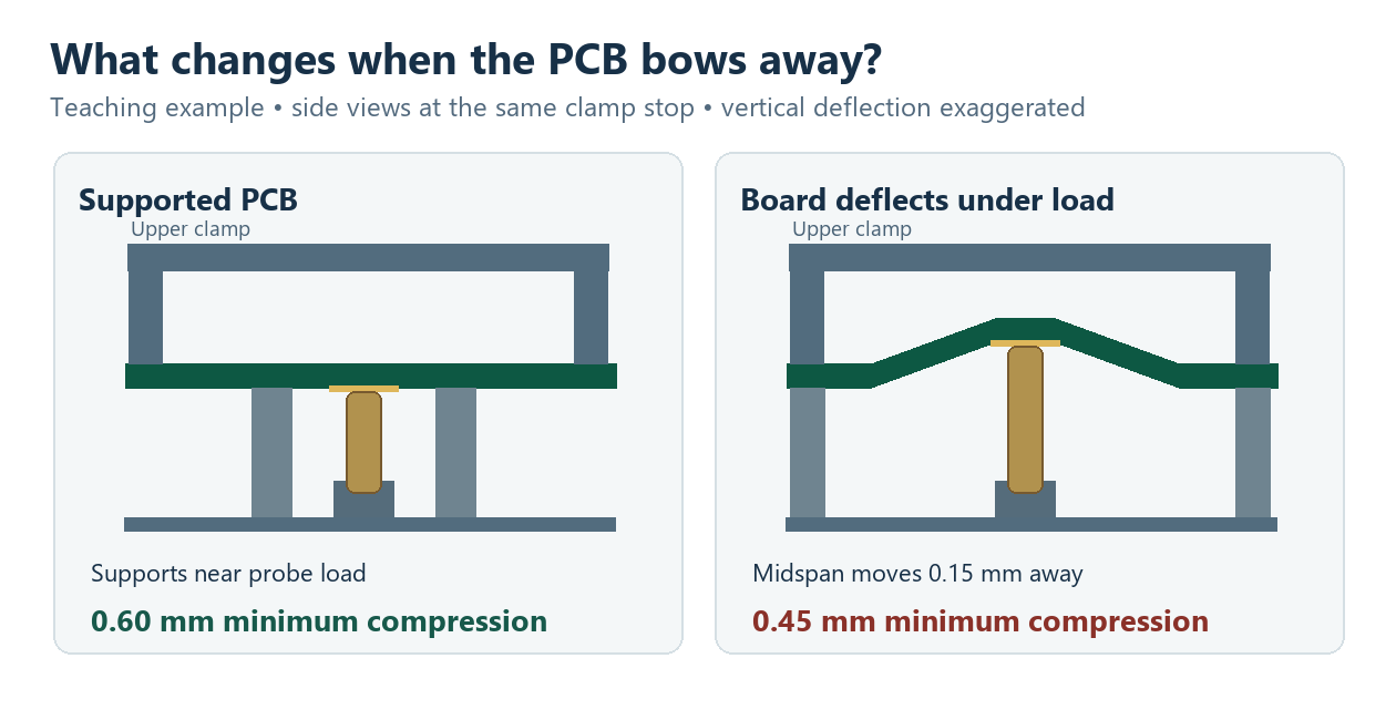
Figure 2. Both clamps close to the same stop. The nearby supports on the left limit travel lost to board deflection. The deflection on the right is exaggerated for clarity.
When there is no safe support area near the probes, compare moving a support or clamp with moving the pad group on the next PCB revision. Fixture changes can require machining and a fresh validation run. Moving pads may affect routing and mask clearances and requires a new board revision. Use loaded measurements before choosing which change to make.
Verify the Fixture Across Repeated Loads
Record Connection, Programming, and Verification Separately
Use a known-good assembled board and a known-good programmer setup as the baseline. Load, close to the stop, run the operation, and fully unload the board. Repeat across representative boards, operators, and fixture positions as applicable. Agree on the number of runs and acceptance criteria before the pilot, based on the production risk and expected variation.
For each cycle, record whether the programmer detected the target, whether it completed programming, and whether the supported verification operation passed. Record the board revision, fixture and firmware versions, and the failure stage. In read-protected workflows, document the supported verification method and when security settings are applied.
Use the Failure Pattern to Choose the First Check
| What you observe | First check | What to compare |
|---|---|---|
| The same pad loses contact on different boards | Inspect the witness mark if the tip leaves one. Check the tip, its wiring and its position relative to the opening. | Compare with a working channel under the same seated condition. |
| Several pads at one end drop out together | Measure compression at both ends with an assembled board seated. Inspect the supports and clamp parallelism. | See whether restoring support or alignment recovers travel and contact in those channels. |
| Contact worsens over successive loads | Inspect the tips for residue or wear and check that the nest still seats the board consistently. | Follow the probe supplier’s cleaning or replacement guidance and retest the same board. |
| The target connects but programming or verification fails | Read the stage-specific log. Check target voltage during the operation, then verify the image, device settings, and relevant signal paths. | Compare against the known-good setup and reproduce the failure at the same stage. |
For review, send the marked pad coordinates, fixture and probe revision, closed-stop travel limits, and pilot logs together. This lets the fixture builder trace a failed cycle back to a pad, a load condition, or an electrical step. See GreatPCB’s PCB assembly testing overview for checks that can accompany the programming operation.
Related Posts

PCBA Prototype
November 19, 2026
PCBA Prototype
October 23, 2026
PCBA Prototype
October 19, 2026