Flex PCB Stiffeners: Materials, Thickness and Design Guidelines
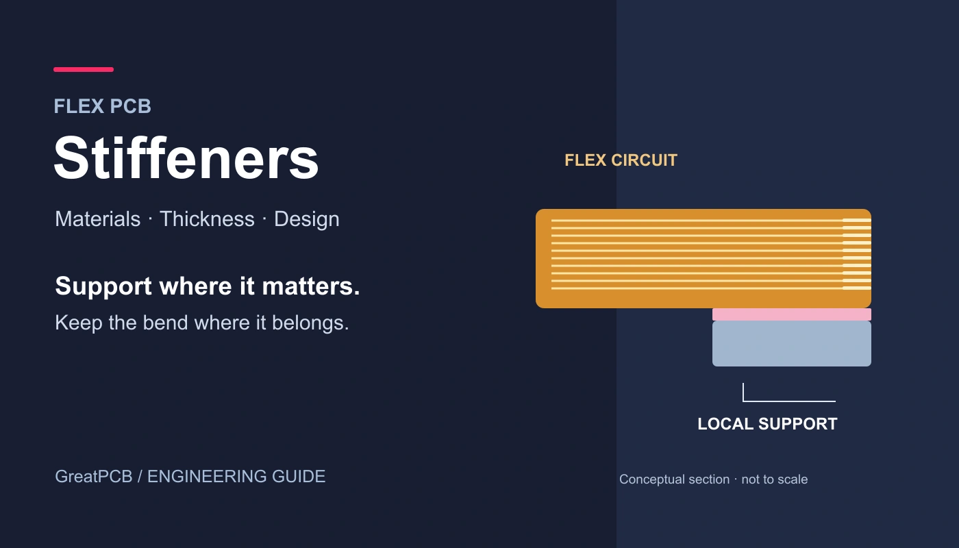
A flexible circuit may need to bend along its cable section while remaining firm under a connector or a group of components. A flex PCB stiffener provides that local support. Choosing one means matching its material, thickness and location to the job the supported area must perform.
For a connector tail, the key dimension is often the finished insertion thickness. Under components, rigidity and assembly access matter more. In both cases, the adhesive and the position of the stiffener edge affect whether the design will work as intended.
What Is a Flex PCB Stiffener?
A flex PCB stiffener is a reinforcing piece bonded to a selected area of a flexible circuit. It increases local thickness or rigidity without making the entire circuit rigid. Common uses include supporting connector contacts, component mounting areas and mechanical attachment points.
Consider a flexible tail entering a connector. The tail must fit the connector’s specified thickness range and remain manageable during insertion. A stiffener can build up that area. Beneath a populated section, reinforcement can instead help limit bending around component joints during handling and installation.
A stiffener is usually a mechanical support rather than a routed circuit layer. Bonding an FR4 piece to a flex circuit therefore does not create the same construction as a rigid-flex PCB, whose rigid and flexible circuit regions are integrated into its electrical stack-up.
Which Stiffener Material Should You Choose?
Start with the function of the reinforced area. Materials that solve a connector-fit problem may not provide the rigidity needed beneath a larger component or mounting point.
| Material | Typical purpose | Main design consideration |
|---|---|---|
| FR4 | Rigid support beneath components, connectors or attachment areas | Available space, added thickness, hole alignment and soldering access |
| Polyimide (PI) | Thin reinforcement and thickness build-up, including connector tails | Finished local thickness, adhesive contribution and required flexibility |
| Metal, such as stainless steel or aluminum | Support where stiffness, available height or a specific mechanical or thermal requirement justifies it | Electrical isolation or grounding, edges, bonding and thermal behavior |
FR4 Stiffeners
FR4 is useful when a region needs substantial mechanical support. Beneath a component area, it helps resist local bending; near a connector, it can help support the assembly against handling loads.
Its position must still suit the assembly. A solid backing piece may be practical beneath surface-mounted components, but a through-hole connector can require openings for leads and soldering access. Holes in the flex and stiffener also need compatible sizes and registration tolerances. Reinforcement should support the joint area without blocking the operation needed to make or inspect those joints.
Polyimide Stiffeners
PI reinforcement is particularly useful where a thin build-up is needed, such as behind the exposed contacts of a flexible connector tail. The required PI thickness follows from the connector interface and the layers already present at that location.
PI used as a stiffener and PI used as coverlay have different jobs. Coverlay protects and insulates circuitry; a reinforcing layer adds the specified local support or thickness. Their shared material name does not make them interchangeable in the drawing or thickness calculation.

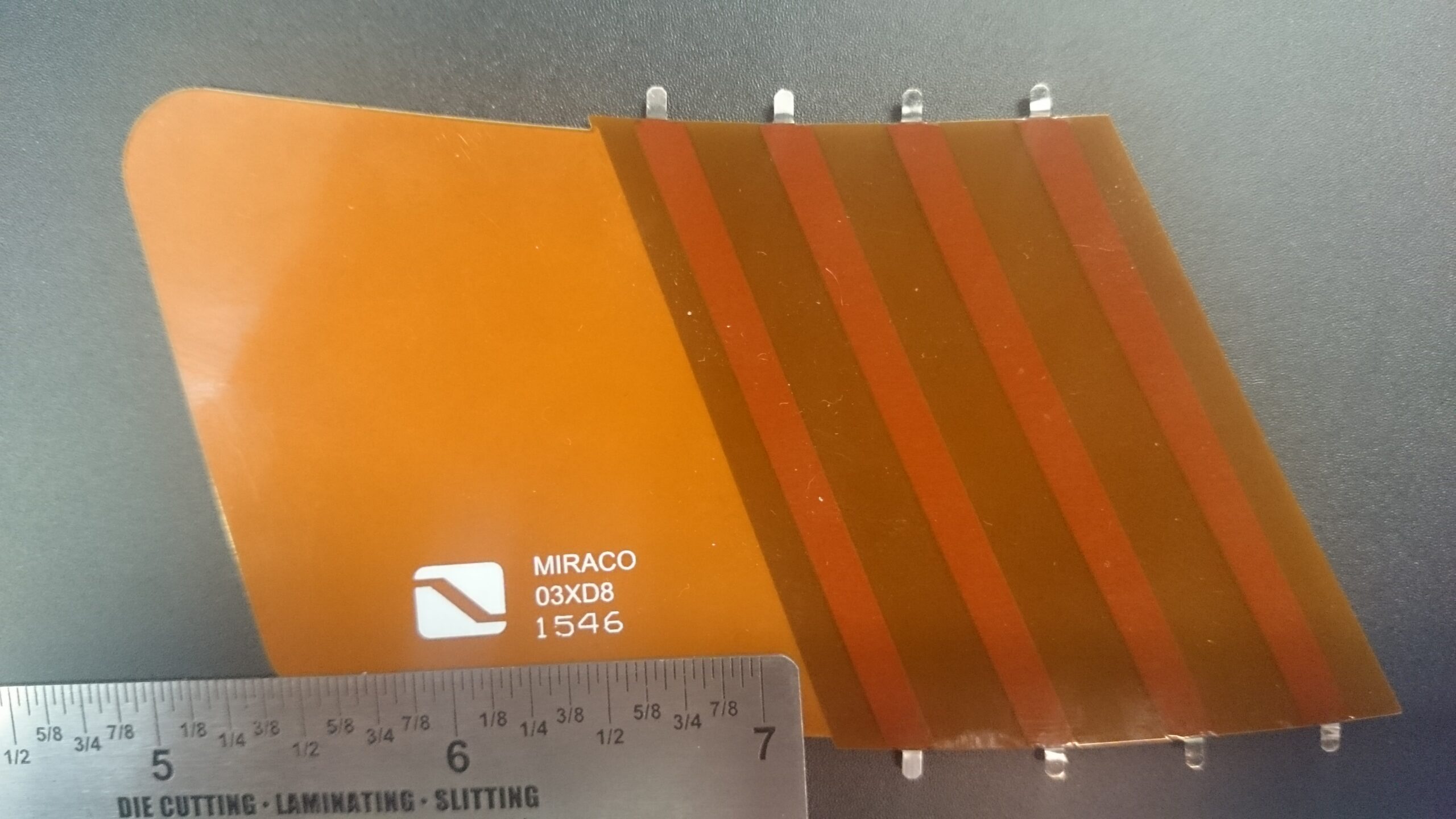
A flexible circuit with a reinforced contact end, from the existing GreatPCB media library. The material and finished thickness must be defined by the drawing.
Metal Stiffeners
Metal can be appropriate when the mechanical design needs a relatively thin, stiff support. Its suitability depends on the alloy, thickness, shape, attachment method and available fabrication processes.
Because metal is conductive, the design must define isolation or an intentional electrical connection. Nearby exposed conductors, edge clearances and assembly hardware all matter. A metal stiffener may also participate in a thermal design, but it should not be called a heat sink simply because it is metal: the heat path and bond layer must support that function.
The stiffener material and its adhesive should be selected together. A suitable reinforcing material bonded with an unsuitable adhesive can still fail the assembly or operating conditions.

Existing site photograph of flexible circuits with local reinforcement. A metal plate requires its own bonding and electrical-isolation assessment.
How Do You Choose Stiffener Thickness?
Three dimensions need separate names: stiffener material thickness, finished adhesive bondline thickness, and finished thickness of the reinforced circuit. Confusing them can produce a tail that looks correct on the drawing but does not fit its connector.
Finished Thickness at a ZIF Connector
For a zero-insertion-force (ZIF) connector, begin with the selected connector’s drawing and its permitted finished cable thickness. Check contact orientation and insertion geometry as well as thickness.
Then establish the flex thickness at the actual contact region. A general board thickness may include layers absent from that region: coverlay can be opened over the contacts, and copper distribution can differ between the tail and the rest of the circuit. The calculation must represent the local construction, including the applicable surface finish.
For a simple stack-up:
Finished tail thickness = existing local flex thickness + finished bondline + stiffener material thickness.
If an adhesive-backed reinforcement is specified by a combined thickness, separate its contributions before calculating. Adding the adhesive again would count it twice.
A Worked Stack-Up Example
The following values are hypothetical assumptions for a design calculation, not specifications for a particular connector or a statement of GreatPCB’s available materials or tolerances.
Assume a connector accepts a finished tail of 0.300 ± 0.030 mm, or 0.270–0.330 mm.
| Contribution | Assumed nominal thickness | Assumed tolerance |
|---|---|---|
| Existing local flex, including all layers present at the insertion area | 0.100 mm | ±0.010 mm |
| Finished adhesive bondline | 0.025 mm | ±0.005 mm |
| Trial PI stiffener material | 0.175 mm | ±0.010 mm |
| Combined stack | 0.300 mm | ±0.025 mm, worst-case addition |
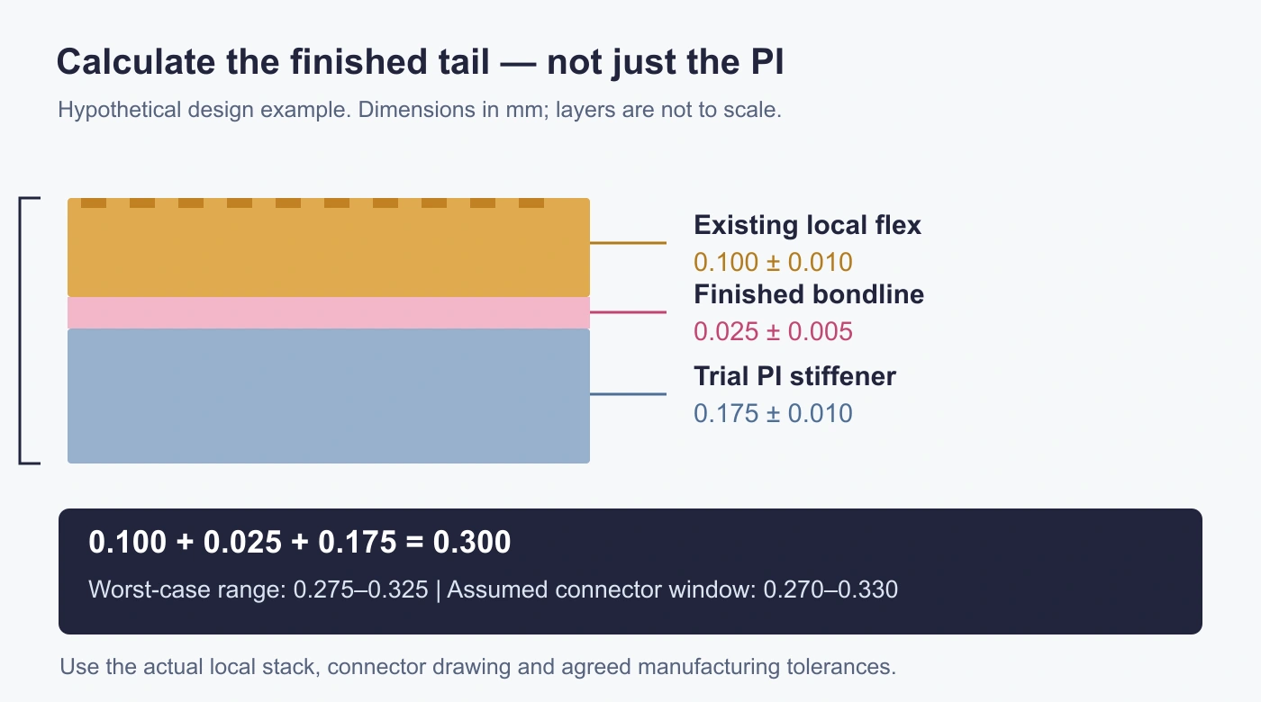
Hypothetical stack-up: the finished connector-tail thickness includes the actual local circuit, bondline and stiffener. Not to scale.
The nominal calculation is 0.100 + 0.025 + 0.175 = 0.300 mm. Adding the assumed tolerance limits gives ±0.025 mm, producing a calculated range of 0.275–0.325 mm.
That range fits within the assumed connector window, with only 0.005 mm remaining at each limit. It is a reason to examine the inputs carefully, rather than treating the nominal sum as sufficient. Available material constructions, finished adhesive thickness and the supplier’s achievable tolerances must replace these assumptions before release. Agree where and how the finished thickness will be measured.
This is a simple worst-case dimensional check. It does not establish production yield, insertion durability or electrical contact performance.
Where Should the Stiffener Go, and How Is It Bonded?
Material and thickness define the reinforcement in cross-section. Its outline and bonding position determine how it interacts with components, soldering and bending.
Position the Support Around the Assembly
For a surface-mounted component area, backing the flex can limit movement beneath the joints. For a through-hole part, the design must also preserve the space needed for lead protrusion and soldering. Connector bodies, mounting hardware and enclosure features can impose additional openings or height limits.
The stiffener edge creates a transition between a supported region and a more flexible region. Define the intended bend location and bend radius so that handling does not repeatedly force the circuit around an unintended sharp transition. A region that flexes repeatedly needs a different assessment from a bend made once during installation.
There is no single edge distance that suits every stack-up, connector and bend requirement. Show the intended bend area and stiffener outline together so their relationship can be reviewed.
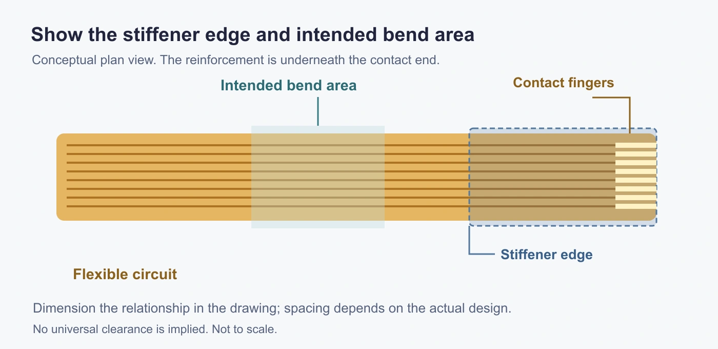
Show the intended bend area and the stiffener edge on the same drawing. Their spacing depends on the actual construction. Not to scale.
Match the Bonding Method to the Process
Pressure-sensitive adhesive (PSA) and heat-activated bonding systems offer different processing routes. PSA bonds through applied pressure under suitable surface and application conditions. Heat-and-pressure bonding can help an adhesive flow and wet the surfaces; a thermosetting adhesive also needs the specified cure. The reinforcing sheet itself is not being melted onto the circuit.
Whether a separate cure or post-bake is needed depends on the adhesive system and process. A generic temperature-and-time recipe should not be applied to every PI, FR4 or metal stiffener.
Likewise, PSA is not automatically unsuitable for every reflow application. For example, 3M describes its 9077 tape for high-temperature applications, including solder reflow. That is a product-specific example, not approval of every PSA or every bonded assembly. Check the actual adhesive against the planned thermal exposure, surfaces and loading.
Bonding sequence also needs consideration on double-sided assemblies. A published double-sided FPC assembly example describes how a local step associated with reinforcement interfered with stencil contact and solder-paste printing. The practical lesson is to review printing and support geometry before fixing the stiffener attachment sequence.
Does a Stiffener Replace an Assembly Carrier?
A stiffener normally remains in the finished product. An assembly carrier is temporary tooling used to support and locate the flexible circuit during manufacturing. They can be needed on the same job.
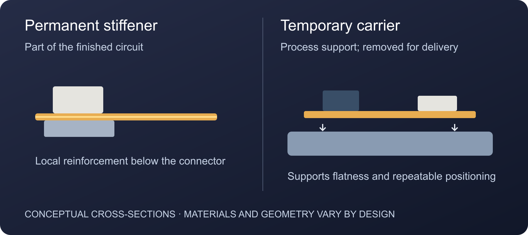
A stiffener remains with the circuit; a carrier supports manufacturing and is removed. Conceptual sections, not to scale.
A tail reinforced for connector insertion may still leave a large, unsupported component area. Conversely, a carrier can support the circuit through printing and placement without providing the permanent reinforcement needed when the product is installed.
During flex PCB assembly, the support plan must account for the whole circuit: where it is located, how the stencil meets the surface, whether tooling clears existing parts, and how the assembly is released afterward. Local stiffeners do not automatically make the remaining flex self-supporting.
Evaluate the finished product’s mechanical needs and the production tooling together. This helps avoid adding permanent material merely to solve a temporary manufacturing problem, or expecting temporary tooling to protect joints after delivery.
How to Specify Stiffeners in Your Fabrication Files
The fabrication drawing should let the manufacturer identify what to attach, where to attach it and which finished dimensions matter. A note that only says “add PI stiffener” leaves several decisions unresolved.
| Drawing item | Information to define |
|---|---|
| Material | Reinforcing material and any required grade or agreed construction |
| Location and side | Dimensioned outline, attachment side and relationship to circuit features |
| Thickness | Material thickness and tolerance; separate finished local total thickness where fit matters |
| Adhesive | Specified or supplier-proposed bonding system, with finished bondline accounted for |
| Openings and alignment | Holes, cutouts, datum references and registration requirements |
| Assembly constraints | Soldering access, component clearances, thermal exposure and intended bend area |
| Verification | Measurement location and acceptance requirements for critical finished features |
For the hypothetical connector-tail example above, an illustrative drawing note could read:
Reinforce the connector-tail area on the side shown. Finished insertion-region thickness: 0.300 ± 0.030 mm, including the local circuit, adhesive and reinforcement. Supplier to propose and confirm the PI/adhesive construction before manufacture. Stiffener outline and inspection area as dimensioned.
That note still requires an actual drawing with the outline, side and measurement area. It deliberately specifies the functional finished dimension while leaving the proposed material combination subject to confirmation.
Cost also follows the construction. Multiple thicknesses, separate pieces on both sides, intricate cutouts and tighter registration can add preparation, positioning or inspection work. Simplify these features where the product permits, rather than assuming one material is always the cheapest. Include the agreed reinforcement construction in the FPC assembly plan so material preparation, tooling and soldering sequence use the same design assumptions.
FAQs
Does Every Flex PCB Need a Stiffener?
No. Reinforcement is needed where the mechanical or interface requirements call for it. A circuit supported by its enclosure may not need the same reinforcement as an exposed connector tail or an unsupported populated area. Review the installed condition and handling loads before adding material.
Is a Flex PCB with FR4 Stiffeners the Same as Rigid-Flex?
No. FR4 reinforcement provides mechanical support; it does not by itself add the electrically integrated rigid circuit regions of a rigid-flex construction. The fabrication drawing should identify which construction is required.
Can a Stiffener Be Added After PCB Fabrication?
It may be possible if the design leaves access for positioning and bonding, and the adhesive process is compatible with the circuit and any installed components. Check finished thickness, holes, clearances and inspection requirements before changing the process. Removing or replacing an existing bonded stiffener can damage the flex, so rework should not be assumed to be straightforward.
Table of Contents
- What Is a Flex PCB Stiffener?
- Ndi Zinthu Ziti Zolimba Zomwe Muyenera Kusankha?
- Kodi Mumasankha Bwanji Kukhuthala kwa Stiffener?
- Kodi Stiffener Iyenera Kupita Kuti, Ndipo Imagwirizana Bwanji?
- Kodi Chokometsera Chomangirira Chimalowa M'malo mwa Chonyamulira Chomangira Msonkhano?
- Momwe Mungatchulire Ovuta mu Mafayilo Anu Opangira
- Ibibazo
Related Posts
PCBA Prototype
October 19, 2026