High-Frequency PCB Material Selection Guide
Select high-frequency PCB materials by matching a complete board construction to your electrical, environmental and manufacturing requirements. Start with the operating band, signal-path length, loss and phase limits. Then compare laminate data under compatible test conditions, check the copper and stackup, and validate a representative prototype.
A material’s Dk and Df help you build a shortlist, but they cannot qualify the finished circuit on their own. Foil, dielectric thickness, bonding layers, surface finish and fabrication tolerances also shape its response.
This guide follows that decision process from requirements to RFQ, with a selection worksheet, a hypothetical project example and checks for prototype acceptance.
Define the RF Requirements
Start material selection with the circuit requirements. A laminate should meet the needs of the finished signal path, including its geometry, environment and acceptance tests. A frequency label alone cannot establish suitability.
Frequency and Signal Path
Record the actual RF operating band and the paths that carry it. For digital interfaces, document edge rate and channel requirements separately from clock frequency. Include approximate routed length, transmission-line structure and connectors or transitions that belong in the channel model.
There is no universal GHz threshold at which every design must abandon FR4. Two circuits operating in the same band may have different material needs because their path lengths and performance margins differ.
Loss and Phase Limits
Define acceptable insertion loss across the required band and identify phase-sensitive paths, such as antenna feeds or matched channels. Allocate the board’s share of the system budget before comparing laminate data. State whether a limit applies to a coupon, a routed PCB path or the complete assembly.
Use a short worksheet to make these assumptions reviewable:
| Requirement | What to record |
|---|---|
| Signal | Operating band; digital edge rate where relevant |
| Path | Length, topology, transitions and reference planes |
| Performance | Loss, impedance, phase or delay limits and tolerances |
| Environment | Temperature range, humidity exposure and conditioning |
| Verification | Test structure, method and acceptance criteria |
Operating Conditions
Temperature and moisture can affect dielectric response and RF loss. Include relevant exposure conditions in the selection criteria. Rogers technical discussion
Distinguish operating conditions from assembly temperatures and qualification stresses. Agree which conditions the prototype must demonstrate before approving a material for production.
Read Dk and Df Correctly
Dk describes a material’s relative permittivity; Df describes its dielectric dissipation. Neither number is a complete prediction of a finished RF path. Before comparing candidates, identify what each value represents and whether it answers your design question.
Match the Test Conditions
Compare Dk and Df at relevant frequencies, using compatible methods, material directions and sample conditioning. Record the tested construction too. A material measurement and a value extracted from a fabricated circuit are not automatically equivalent: circuit extraction can respond to copper roughness, plating and gaps as well as the dielectric. These distinctions are explained in Rogers’ overview of Dk and Df test methods.
Create a comparison record with a separate field for each condition. If a supplier lists Df at one frequency and another uses a different method or frequency, mark the comparison unresolved. Ask for comparable data instead of ranking the materials from those two numbers. Also separate a typical property from an agreed purchase specification; your shortlist should state which information still needs confirmation.
Process Dk and Design Dk
The RO4000 data sheet illustrates why labels and footnotes matter. For RO4350B, it lists process Dk of 3.48 ±0.05, measured by clamped stripline at 10 GHz and 23°C, and design Dk of 3.66, obtained by differential phase length over 8–40 GHz. A footnote gives 3.33 ±0.05 process Dk for the 4 mil material. Read the exact thickness entry rather than transferring one grade-level number to every construction. These form a specific data-sheet example, not a default value for every simulation.
Match the supplier’s Dk definition to your simulator’s treatment of propagation and copper roughness. Bulk material inputs and circuit-calibrated values may account for those effects differently; combining them carelessly can count an effect twice. Do not assume every published design Dk already includes roughness. Rogers discusses this distinction in its fabrication and material considerations for 5G.
Document the chosen input, its source and the model settings alongside the stackup. That makes a later coupon-to-model comparison useful and keeps substitutions reviewable.
Compare Material Families
Use a material family to build a shortlist, then evaluate the exact grade and finished construction. A family name alone does not establish a board’s insertion loss, phase stability or fabrication yield.
FR4 and Low-Loss Laminates
Conventional epoxy-based laminates remain candidates when the finished circuit can meet its electrical and environmental requirements. Compare the actual laminate construction rather than treating “FR4” as one RF material. A short interconnect and a phase-sensitive feed network can require different choices even at the same operating frequency.
Include purpose-formulated low-loss candidates in the shortlist. For example, Isola supplies I-Tera MT40 as laminate and prepreg and describes FR4-compatible processing without special PTFE-like through-hole treatments. That processing description is useful for manufacturing discussions; it does not establish a universal electrical advantage. Check the exact variant before comparing properties. Isola I-Tera MT40.
Hydrocarbon/Ceramic and PTFE Materials
RO4000 materials illustrate hydrocarbon/ceramic thermoset laminates rather than PTFE. RO3000 illustrates ceramic-filled PTFE microwave laminates, with grade-specific properties and copper options. These are different material systems; neither family label selects the right grade for a design. RO4000 data sheet, RO3000 series.
| Candidate | Reason to consider | Limitation to resolve | Verification |
|---|---|---|---|
| Conventional epoxy-based laminate | Candidate for requirements that allow it | Generic FR4 designation lacks sufficient RF detail | Confirm construction and test the intended path |
| Formulated low-loss laminate | Lower dielectric loss with a familiar processing route where supported | Variant and process assumptions need checking | Review its current data sheet and fabrication plan |
| Hydrocarbon/ceramic | Controlled dielectric properties with a thermoset processing route | Family membership does not qualify every grade | Confirm grade, copper and construction |
| Ceramic-filled PTFE | Low-loss microwave paths with grade-specific dielectric behavior | Properties, foil and processing requirements vary by grade | Confirm grade and fabricator experience |
Advance candidates that meet the agreed requirements with a fabrication route the supplier can explain and verify. For a focused two-material comparison, see our Rogers 4350B versus FR4 guide.
Check the Full Construction
A laminate designation is only part of the RF stackup. Compare candidates using the construction you intend to fabricate: dielectric layers, foil, finished conductors, surface finish and solder mask. Material Df describes dielectric dissipation; it does not establish the insertion loss of the fabricated RF path.
Copper and Surface Finish
At high frequencies, skin effect concentrates current near conductor surfaces. Texture at the copper–dielectric interface can therefore affect conductor loss and phase response, even when the laminate grade stays unchanged. Copper choice belongs in the electrical model alongside the dielectric. Rogers discusses these construction sensitivities in its millimeter-wave transmission-line guidance.
Specify the foil type, treated face and roughness measurement method. Ra, Rz and Sq describe different aspects of texture; their reported values are not interchangeable. Ask which surface the measurement represents and whether its definition matches the simulator’s roughness model. Also distinguish starting foil thickness from finished copper after processing. A smooth-foil label alone cannot resolve adhesion, treatment or fabrication requirements.
Include the intended finish on exposed RF conductors and pads. Evaluate it in the relevant geometry rather than applying a universal finish ranking. Solder mask also needs its actual formulation and coverage: its dielectric loading can change RF behavior. Rogers’ solder-mask guidance supports considering these effects during design.
Thickness and Bonding Layers
Changing dielectric thickness changes the line width required for a fixed impedance. A thicker microstrip dielectric generally permits a wider conductor, which can reduce conductor loss, but radiation and other geometry-dependent effects can offset that benefit. A thinner construction can improve some field-control characteristics while requiring narrower traces. Neither direction is automatically better. The tradeoffs also depend on the microstrip or stripline topology.
Make the comparison construction explicit:
- Record finished dielectric thickness and its agreed tolerance.
- Identify every bonding dielectric crossed by the RF fields.
- Include foil, finished copper, finish and mask coverage in the model.
- Carry the same construction into the representative test path.
This prevents a favorable laminate result from being mistaken for the performance of a different finished stackup.

Conductor geometry and surface construction belong in the review alongside the laminate.
Check Environmental Stability
Temperature and Moisture
Electrical suitability must extend beyond the conditions used for the first simulation. The temperature coefficient of dielectric constant (TCDk) describes how dielectric response changes with temperature. That change can shift electrical length and phase. Moisture conditioning can also alter dielectric behavior and RF loss. These effects deserve attention in phase-sensitive feeds, filters and matching networks. Rogers discusses temperature and moisture effects in RF material selection.
Define the conditions the finished board will face: operating temperature range, humidity exposure, enclosure protection and transitions between storage and operation. A dry-room prototype result does not establish suitability for a humid installation. Likewise, a data-sheet moisture absorption value needs its stated conditioning to be meaningful. Use those conditions to identify which material claims require supporting evidence for your application.
Check the direction and magnitude of TCDk over the supplier’s stated temperature interval. A more negative number does not mean less drift; stability concerns how close the response remains to its target. Use grade-specific thermal data, and do not assume two materials with the same resin family have the same temperature behavior.
Expansion and Thermal Paths
TCDk differs from the coefficient of thermal expansion (CTE): one concerns dielectric response; the other concerns dimensional change. Expansion affects mechanical stresses in the board construction. Supplier tables also distinguish glass-transition temperature (Tg), decomposition temperature (Td), thermal conductivity and moisture absorption, sometimes identifying different Tg measurement methods. These properties answer different questions; none independently approves a system service temperature. Isola’s I-Tera MT40 RF/MW properties table illustrates that separation.
For a power-bearing design, review how heat reaches copper, vias, mounting interfaces and the enclosure. Laminate conductivity alone cannot predict component junction temperature. Ask whether the proposed construction supports both the electrical path and the thermal path, then check whether that construction is available and practical to manufacture.
Confirm Manufacturing Options
A promising datasheet becomes a practical choice only when the fabricator can build the intended construction. Review the proposed PCB stackup before routing fixes the layer spacing and via structure.
Available Grades and Thicknesses
Ask the fabricator to confirm the exact material grade, core thickness, copper weight, foil option and bonding layers. Distinguish nominal core dimensions from the finished stackup thickness used in the electrical model. Check current availability and agree on how any substitution will be reviewed before accepting it.
Processing requirements also vary. For example, Isola describes I-Tera MT40 as compatible with FR-4 processing, without the special through-hole treatments associated with PTFE. That does not establish compatibility for every low-loss material or stackup.
Have the fabricator identify any material-specific hole preparation, bonding or pressing requirements relevant to the proposed build. Confirm the manufacturing route for the exact construction rather than assuming that a familiar product family guarantees it.
When a Hybrid Stackup Helps
A hybrid stackup can place selected RF layers on a qualified low-loss dielectric while other layers use another suitable material. It is a layer-by-layer construction, not an arbitrary division of one layer into different substrate zones.
Evaluate compatible bonding and pressing processes, mechanical alignment and the dielectric environment around each critical RF path. Specify which material supports each transmission line and reference plane so the simulation matches the proposed build.
Treat reduced material use as a design option, not a guaranteed cost saving. For additional context, see mixing PCB materials; request approval of the complete hybrid stackup before committing to it.
Use a Selection Matrix
Shortlist the Candidates
Consider a hypothetical RF front-end feed path operating from 5.8 to 6.2 GHz, with nominal impedance of 50 ohms and roughly 60 mm of routed length. Assume the project allows no more than 1 dB insertion loss across the complete path, including its transitions. These are illustrative design requirements, not measured results or general acceptance limits. The system team must also define the phase and environmental requirements.
Use the following matrix to identify the evidence needed for each candidate. A family name alone does not pass any gate.
| Selection gate | Evidence to obtain for each candidate | Decision |
|---|---|---|
| Loss budget | Model and measured response of the complete proposed path | Compare against the 1 dB project target across the band |
| Phase stability | Response under the required conditions, with agreed reference planes | Apply the system team’s phase or delay limits |
| Construction | Exact dielectric, foil, thickness, finish and bonding details | Keep the model and proposed build consistent |
| Repeat production | Available configurations and an agreed fabrication route | Resolve substitutions and process uncertainty |
Test the Tradeoffs
Apply the same gates to a specified conventional FR4 grade and any shortlisted low-loss, hydrocarbon/ceramic or PTFE alternatives. Record unresolved questions and their owners. Missing supplier data or an unavailable foil option remains an open item, not a favorable score. Substituting one generic material value into every model can conceal the actual tradeoff.
Choose the simplest qualified candidate that satisfies all requirements and has an agreed route to repeat production. If a candidate misses the loss or phase budget, investigate whether the cause lies in dielectric behavior, copper, geometry or transitions before moving to a more expensive material. A change should address a demonstrated limitation. Carry the shortlisted construction and its open questions into prototype validation.
Validate the Prototype
Representative Test Paths
Validate the construction with representative paths. Include the planned foil, core thickness, finished copper, trace geometry, solder-mask coverage and surface finish. Where performance depends on a connector launch, via transition or layer change, include that feature in the evaluation.
Material measurements and measurements on fabricated circuits capture different influences. Circuit results can reflect conductor plating, roughness and dimensional differences as well as the dielectric. This is why a laminate certificate and a finished-path measurement serve different purposes. Rogers explains the distinction between material and circuit test methods.
Define the measurement reference planes and calibrate the vector network analyzer (VNA) for the setup. If fixtures or adapters remain between those planes and the test path, account for their response. De-embedding requires suitable characterization and valid models; it does not automatically remove every measurement error. Keysight’s calibration-plane guidance describes this dependence on the measurement arrangement.
Electrical and Environmental Checks
Use separate checks for separate questions:
- Construction: inspect the dimensions and layer arrangement that determine the modeled response.
- Continuity: confirm bare-board connectivity; this does not establish RF transmission performance.
- RF response: compare return loss, insertion loss and phase against the agreed targets across the operating band.
- Environmental response: compare relevant measurements before and after the project’s agreed exposure conditions.
An impedance coupon supports an impedance check; it does not prove acceptable insertion loss or performance throughout the intended operating environment. Temperature and moisture can affect dielectric response and RF behavior, so select exposures relevant to the application rather than applying a universal recipe. Rogers discusses these environmental influences.
Record construction departures before interpreting a failed result as a material failure. Qualify a reproducible board construction and RF path, with evidence to guide the next revision.
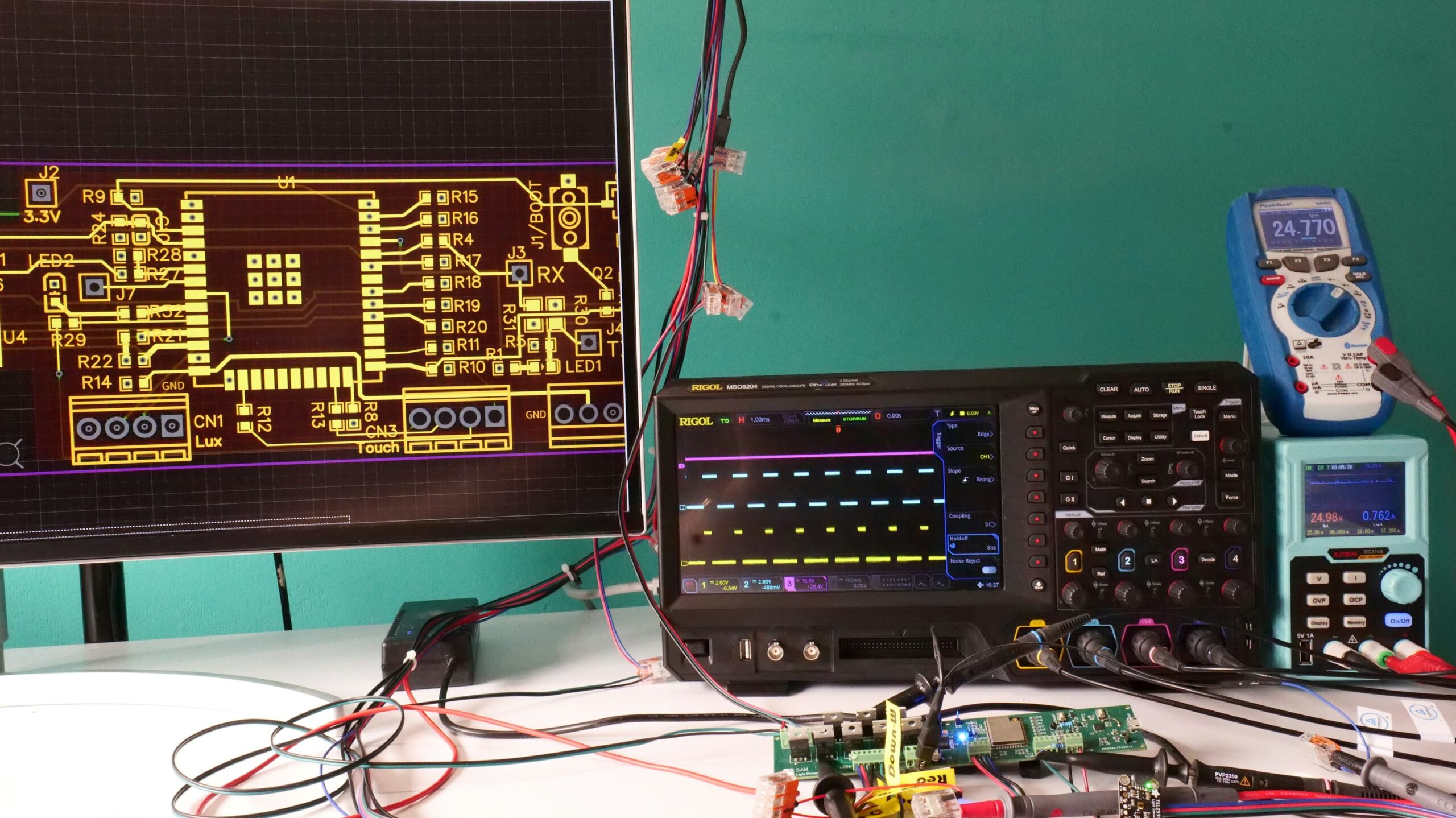
Choose measurements that answer the electrical requirements of the prototype. This illustrative workbench is not a VNA test setup.
Prepare the RFQ
Give the fabricator enough information to quote the construction you intend to qualify. “Rogers PCB” or “low-loss board” leaves important choices unresolved and makes quotations difficult to compare.
Material and Stackup Notes
Provide a coordinated release package:
- Exact laminate grade and applicable data-sheet revision, with approved alternatives listed separately.
- Layer order, core and bonding materials, foil construction, finished dielectric and copper thicknesses, and agreed tolerances.
- Gerber or other agreed manufacturing data, drill files, quantities and delivery requirements.
- Controlled-impedance targets, critical RF paths, and required finish and solder-mask coverage.
Identify which dimensions are fixed by the electrical design and which the fabricator may propose changing. Keep the drawing, simulation and material callouts on the same revision.
Acceptance and Change Control
Separate bare-board inspection requirements from RF performance acceptance. State the test structures, frequency band, reference planes, conditioning, limits and reports needed for the project. Confirm who will perform each check and how results will be reviewed.
Require approval before changing laminate grade, foil, thickness, bonding material or finish where the change could affect the qualified RF construction.
For a GreatPCB quotation, share your files, proposed stackup and material requirements through our high-frequency PCB service, including any RF acceptance or prototype-validation requirements for discussion.
FAQs
Is There a Frequency Limit for FR4?
There is no single cutoff that qualifies every FR4 board. Suitability depends on the exact grade, path length, construction, performance budget and environment. Evaluate the finished path over the required band. A short connection that meets its budget does not qualify a longer antenna feed using the same material.
Which Dk Should I Use?
Use a value whose definition, frequency range and construction match the model you are building. Check the supplier’s test method and the simulator’s treatment of copper roughness. Record the selected input and its source; resolve discrepancies through representative circuit measurements rather than choosing whichever number gives the preferred simulation.
Does Lower Df Guarantee Lower Loss?
Lower Df can reduce the dielectric contribution under comparable conditions. Total insertion loss also depends on conductors, geometry, transitions and the finished surface construction. Compare equivalent paths, and confirm that an improvement in one loss component improves the complete path rather than being offset elsewhere.
Can RF and Digital Layers Use Different Materials?
Yes, a hybrid stackup can assign different qualified dielectrics to selected layers. The bonding system, manufacturing route and reference-plane arrangement must support that construction. Identify every dielectric contributing to each critical RF path, and obtain agreement on the complete stackup before finalizing the layout.
Does an Impedance Test Prove RF Performance?
An impedance check answers a narrower question than RF qualification. It does not independently establish insertion loss, phase stability or behavior after environmental exposure. Define additional measurements around the actual RF path and acceptance requirements; a laminate certificate or bare-board continuity report answers different questions again.
Related Posts
PCBA Prototype
September 8, 2026