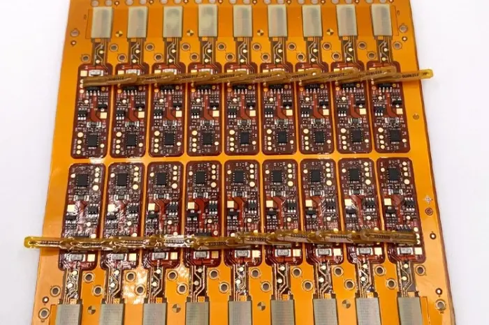
Electromagnetic Compatibility Design for Smartphone PCBs

Have you ever wondered why some electronic gadgets play nice in all sorts of electromagnetic environments while others get twitchy, drop signals, or even behave erratically? That’s down to electromagnetic compatibility, or EMC for short—the ability of a device to both tolerate external electromagnetic “noise” and keep its own emissions under control so it doesn’t bug the neighbors. Let’s dive into some practical, down-to-earth tips for designing PCBs that behave themselves in the real world.
1. Pick the Right Trace Width
When a fast transient pulse shoots down a PCB trace, the biggest culprit for unwanted “kickback” interference is the trace’s inductance. Here’s the quick fix: keep your traces short and fat wherever you can. Inductance scales up with length and down with width, so a short, wide run of copper is your best friend.
Clock lines, bus drivers, and any place you know big edge-rate currents will show up? Keep those traces as short as humanly possible.
For through-hole parts or discrete circuits, around 1.5 mm width is usually plenty.
For surface-mount ICs or finer-pitch work, you can go as narrow as 0.2 – 1.0 mm, but remember: the wider, the lower the inductance.
The bottom line: if you expect hefty current spikes, give them a chunky, stubby highway, not a skinny country lane.
2. Adopt a Smart Routing Strategy
Sometimes you’ll hear “use equal-length routing” to reduce loop area and minimize inductance—and that’s true to an extent—but if you wire every trace the same way on one layer, you’ll end up with massive mutual inductance and extra capacitance between them. That can bite you with crosstalk and slower edges.
A better trick—if your layout can handle it—is a grid (“tic-tac-toe”) mesh approach:
One layer runs horizontal, the next runs vertical.
At each crossover, you stitch them together with plated vias.
This gives you controlled trace geometry and helps distribute return currents neatly, cutting both inductance and unwanted coupling.
3. Keep Crosstalk in Check
Crosstalk is when signal A “whispers” into signal B, and it’s the bane of anyone packing signals tightly together. To tame it:
Avoid long parallel runs of high-speed lines.
Space out aggressive signal pairs—clock, bus, LVDS lanes—away from each other whenever possible.
Never cross a signal line over a power or ground trace; that makes weird, unexpected loops.
For super-sensitive nets, slip a grounded trace between them like a diplomatic envoy; that grounded “guard trace” will soak up coupling and keep them from gossiping.
Spacing, spacing, spacing—that’s the mantra for quiet circuits.
4. Minimize Radiated Emissions
When you slam a fast edge down a trace, it behaves like an antenna, radiating energy out into space. To keep your board from turning into a Wi-Fi jammer, follow these pointers:
Smooth out your traces. Minimize abrupt width changes or 90° bends—those corners act like little antennas. If you must bend, use gentle curves or 45° angles.
Clock nets are notorious emitters. Route clock lines close to their ground return plane—ideally sandwich them between two reference planes—and keep the driver chip right next to the board connector.
Bus drivers belong right up against their bus connector, especially if those lines leave the PCB entirely. The shorter that lead, the less it radiates.
Interleave data lanes with ground. For every two data lines, stuff a ground line between them. Bonus points for hugging the least critical address lines with ground because those address nets can carry nasty high-frequency edges.
Partition by speed. When you’ve got a mix of high-, medium-, and low-speed logic, cluster them: put the high-speed gang together in one corner, the medium-speed crew in another, and the slow folks off in their own little cul-de-sac. That way, the riskiest edges stay far from the chiller nets.
5. Suppress Reflections with Termination
Ever get weird glitches or ringing at the end of a long PCB trace? That’s a reflection—like an echo in a hallway—bouncing back down the line. You can fight it a few ways:
Shorter is sweeter. If you can keep your traces under 10 cm for a medium-speed TTL or CMOS signal, reflections usually stay manageable.
Slow down your edges. Using a driver with gentler slew rates cuts down the high-frequency content that reflects.
Add termination resistors. At minimum, stick a resistor equal to the trace’s characteristic impedance at the far end, tied to either ground, VCC, or a Thevenin divider. For TTL speeds above about 10 MHz, consider source termination (in series at the driver) or parallel termination at the receiver.
Pick your resistor value based on the driver’s output drive current and the highest sink current you expect. A little math goes a long way here in taming that ringing.
6. Embrace Differential Pairs
If your board’s got super-fast or noise-sensitive signals—USB, Ethernet, LVDS, PCIe, you name it—the differential pair is your secret weapon. Two tightly coupled traces carrying equal-and-opposite voltages will radiate far less and tolerate more external noise than single-ended lines.
To do it right:
Maintain equal length to within a few mils. Any mismatch turns your neat differential wave into a radar dish.
Keep the spacing between the pair constant along the entire run. That spacing determines the pair’s differential impedance (50 Ω, 100 Ω, whatever your standard calls for).
Pack the pair close together, but leave enough room so your board shop can etch it reliably. A tight, consistent gap ensures the fields around each trace cancel each other, cutting EMI.
Follow your high-speed rules—layer transitions, return paths, and via stubs all matter for that pair’s signal integrity. Every jog, twist, and via adds complexity, so plan your route carefully.
Bringing It All Together
EMC isn’t just a checkbox—it’s about making a robust, reliable board that plays nicely with everything around it. By minding trace inductance (width and length), adopting smart routing patterns, spacing for crosstalk, guarding against radiation, terminating to kill reflections, and riding the differential wave, you’ll be well on your way to a PCB that sails through compliance testing and keeps customers happy.
So next time you fire up your layout tool, remember: a few millimeters here, a grounded guard trace there, and the right resistor at the end of that bus line can make all the difference between a board that whistles Dixie and one that marches to the tune you intended. Happy routing!
Table of Contents
Related Posts
PCBA Prototype
April 13, 2026
PCBA Prototype
April 10, 2026


