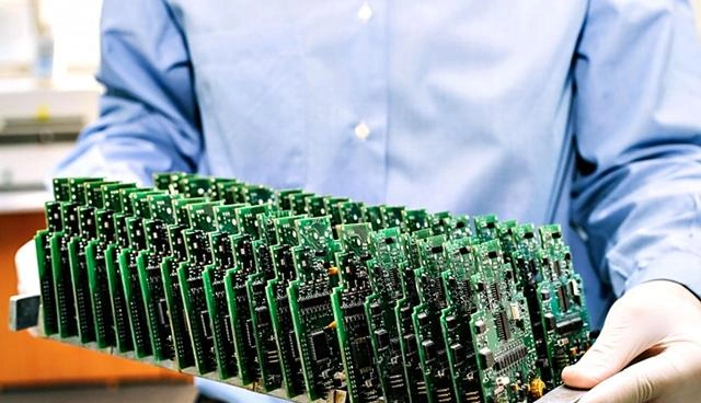
Optimize PCB Costs: Component Selection to Fabrication

1. Cost Control in the Design Phase
(a) Picking the Right Components
You know how sometimes engineers go for the fanciest, highest‑spec parts just to be on the safe side? Well, that can really jack up your bill of materials. Take a typical smart wristband: its job is just step‑counting, heart‑rate monitoring, and basic notifications. You don’t need a blazing‑fast microcontroller for that—mid‑range chips handle it just fine. In fact, swapping out a top‑end MCU for a mid‑range one can shave off roughly 30–40% of the component cost. Scale that to a production run of tens of thousands, and you’re talking serious savings. Plus, high‑end parts often demand fancier power circuits and more robust heat dissipation, which adds even more complexity and cost on your PCB. Bottom line: figure out exactly what performance your product needs, then match your parts to that—no more, no less.
Opt for Commodity Parts First
Commodity parts are like the bread and butter of electronics—they’re everywhere, they come in standard packages, and they’re usually a bargain. Think 0402 or 0603 resistors and capacitors: almost every factory stocks them. If you stick with common specs, you can pay 20–30% less than you would for custom or exotic parts. And if your supplier hits a hiccup, you can quickly source replacements elsewhere—no production line stoppages. I once heard about a company that used a weird, special‑order capacitor; when that supplier ran into production trouble, the whole board line stalled for weeks. Ouch. So unless your design absolutely calls for a bespoke part, stick with the stock‑room staples.
(b) Fine‑Tuning PCB Size and Layer Count
Nailing Down Dimensions
In the early PCB layout stage, getting your board size right is like laying a solid foundation for a building. Board area drives the raw material cost, which is often a hefty slice of the overall PCB price. Engineers should dive into the product’s mechanical design: where does each module sit? How much room do you actually have? For example, a small Bluetooth speaker’s guts are tight. By hugging the audio, power, and BT modules close together, you can trim board size by around 10%. If you’re making 100,000 units a month, and each board costs about $0.70 in raw laminate, that’s a $7,000 monthly saving right there. Smaller boards can also mean shorter trace runs, which cuts down on signal loss—and assembly machines can work more efficiently when there’s less empty real estate to navigate.
Choosing the Right Layer Count
Every extra layer on a PCB comes with a price tag. Jumping from two layers to four can hike cost by 50–80% because you’re paying for more laminate and more processing steps. So don’t just say “more layers are always better.” For a simple control board in a home appliance, two layers often suffice: one for power, one for ground, and vias stitching things together. But if you’re pushing megahertz or gigahertz‑level signals—like in 5G gear—you might need more. In those cases, simulate different layer stacks with signal‑integrity tools. We’ve seen projects where a six‑layer stack hit performance targets, but going to eight layers only added cost without clear benefits—costing 30% more in manufacturing without a big bump in signal quality.
(c) Smarter Layout and Routing
Follow Functional Zoning
Think of your PCB like a city: group together components that “live” in the same neighborhood. Put the power‑management chip next to its decoupling caps and inductors, rather than scattered across the board. In a 5V‑to‑3.3V regulator, that can cut trace lengths from centimeters down to millimeters—saving copper, reducing parasitics, and boosting efficiency. Short traces mean less signal degradation and noise. Plus, when something goes wrong, technicians can zero in on one zone instead of scouring the whole board.
Keep Traces Direct and Simple
Avoid meandering, curly‑cue traces. Every extra 1 mm of trace adds resistance, inductance, and potential crosstalk. For high‑speed signals, impedance matters, so choose trace width and spacing carefully. Don’t be overly conservative—if your signal‑integrity analysis shows you can get away with 6 mil width and 8 mil spacing at 1 GHz, go for it, instead of the 10/12 mil you might have defaulted to. That’s more real estate for routing and sometimes means fewer layers are needed. Also, don’t leave big empty blank spots. Tighten things up so you make the most of your board area—sometimes you can sneak in another feature or boost reliability at no extra cost.
2. Material‑Choice Cost Considerations
(a) Zero in on Performance Needs
Different products dance to different tunes. A cheap kids’ toy deals with low‑frequency signals; the odds are high‑speed data integrity isn’t mission‑critical. In those cases, FR‑4 laminate does the job: it’s mechanically sturdy, electrically insulating, and cheap—often 50–70% less expensive than fancy high‑frequency substrates. On the flip side, aerospace or radar gear might need PTFE or ceramic substrates with ultra‑low dielectric loss. But those can cost multiple times what FR‑4 does. So match your laminate to the environment and the signal speeds you’re pushing.
(b) Weigh Material Specs Against Price
Say you’re choosing between aluminum‑based and copper‑based clad materials for an LED driver board. Aluminum boards conduct heat well and are relatively inexpensive—ideal for cost‑sensitive products that still need some heat‑dissipation oomph. Copper‑base is even better at spreading heat and has slightly superior electrical properties, but it comes with a heftier premium. Collect quotes from multiple suppliers, gather sheet‑resistance, thermal conductivity, and price data, then crunch the numbers in a simple performance‑vs‑cost model. In one example, an LED driver at 10 W ran just fine on a mid‑grade aluminum board, saving about 30% over copper clad.
(c) Check Compatibility, Not Just Cost
A low‑cost material that can’t handle your soldering temperatures is a false economy. If you’re doing wave solder, you need resin/glass transition temperatures (Tg) well above your peak process heat. Otherwise your board warps or delaminates. Also consider chemical compatibility: some flux residues can corrode thin metal finishes if the substrate’s chemistry isn’t tuned for it. When picking surface finishes or coatings, make sure they play nicely with your component leads too, or you’ll risk bad joints and rework costs down the line.
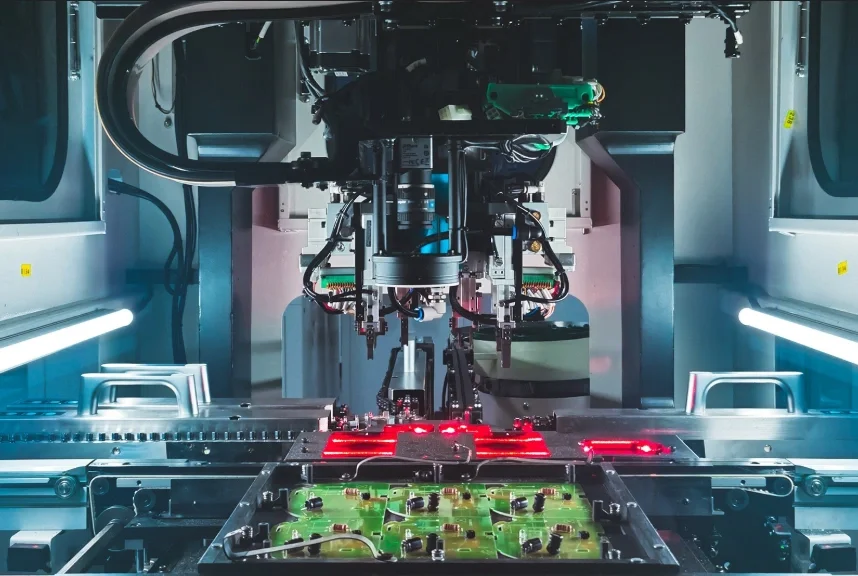
3. Manufacturing‑Process Cost Optimization
(a) Design for Manufacturability (DFM)
Respect Process Capabilities
Component pitch matters. If parts are too close, pick‑and‑place machines can’t grab them cleanly, leading to mis‑picks and run‑offs. Data shows yields can drop by 20–30% and throughput by 30–50% if you push spacing below the machine’s sweet spot. Chat with your contract manufacturer early to learn their nozzle clearances and fiducial requirements. They’ll tell you the min‑spacing that keeps production smooth.
Via Design Matters
Make vias neither too small nor too big. Too small, and plating can clog them; too big, and you waste routing real estate. Clogged vias can bump defect rates by 10–15%. Also, sprinkle in test‑point vias or pad markers where your in‑circuit testers can probe. A well‑placed test network can lift yield by 15% and cut debug time by 20–30%.
(b) Team Up with Your Fab
Know Their Cost Drivers
Early on, forge a dialogue with your PCB shop. They know which panel shapes minimize waste, which drills drive up costs, and how certain dimension tolerances affect pricing. For instance, laser‑drilled microvias are great for HDI boards but cost way more than mechanically drilled holes. If you don’t need them, skip ’em.

Volume Discounts & Long‑Term Deals
Buying 10,000 boards a month may get you basic pricing, but if you can commit to 50,000 a month or a year‑long contract, you might snag 10–20% discounts. And when raw‑material prices swing, a long‑term partner will often prioritize your orders or offer buffering clauses so you’re not paying peak rates every time.
(c) Balancing Quality and Cost
You can’t sacrifice quality entirely, but neither should you over‑inspect. For incoming laminate and parts, use sampling methods—bump up sample rates on critical lots, but scale back on mundane items. On the line, in‑process monitors (like automated optical inspection) can catch defects in real time; use them, but tune them so they don’t flag every minor spec drift that’s still within tolerance. Overly harsh reject criteria can whisk out perfectly acceptable boards, inflating scrap rates and costs. Finally, final electrical tests and a quick visual check before shipping will catch any stragglers.
Wrap‑Up
Cost control isn’t a one‑time checkbox; it’s a thread woven through design, material selection, and manufacturing. By choosing appropriately specced components, optimizing board size and layers, zoning and routing smartly, and collaborating tightly with fabricators—while balancing quality checks—you can squeeze every drop of efficiency out of your process. Do that, and you’ll see margins swell without compromising performance or reliability.