Double Side PCB
FR4 standard
Assembly

What is a double sided PCB?
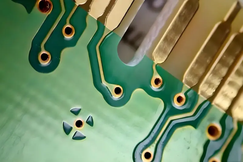
Double-sided printed circuit boards have double-sided wiring,having the top and bottom floors. All surface treatments can be achieved, all types and colors of weld resistance layers, including matte and gloss. Double-sided printed circuit boards are mounted with conductive copper and components on both sides of the printed circuit boards so that the wires can cross each other. It results in higher density of circuit boards without point-to-point welding, making double-sided printed circuit boards is difficult, complex, and better using double-sided than single-sided printed circuit boards.
The Versatility of Double-Sided PCBs
Double-sided printed circuit boards are one of the most popular PCB types because they enable manufacturers to make more complex circuits, which benefit higher-tech applications and electronic products. Double-sided printed circuit boards can be used in a variety of applications and electronic products, such as: LED lighting systems, vending machines,amplifiers, automotive dashboards, industrial controls, telephone systems.

how to solder double sided pcb
The main methods for soldering double-sided PCBs include selective soldering and reflow soldering. The specific steps are as follows:
Selective Soldering:
- Flux Application: Before soldering, apply flux to the circuit board to prevent bridging and oxidation. The flux application should be carried out by an X/Y robotic arm that moves the circuit board above the flux nozzle, ensuring that the flux is evenly coated on the soldering points of the circuit board.
- Microwave Peak Soldering After Reflow Soldering Process: It is crucial for the solder to be accurately sprayed. The diameter of the micro dot flux application should be greater than 2mm, and the position accuracy of the flux deposited on the circuit board should be ±0.5mm to ensure that the flux consistently covers the soldering area.
- Process Characteristics: The main difference between selective soldering and wave soldering is that in selective soldering, only specific areas come into contact with the solder wave, while the circuit board itself acts as a poor thermal conductor, preventing the solder points near components and circuit board areas from melting.
Reflow Soldering:
For reflow soldering of double-sided boards, different methods can be employed, including:
- Solder Paste on One Side and Red Glue on the Other: This method is suitable for densely packed components on one side with varying heights. The red glue provides more stability for large components under significant gravity. The process flow includes applying solder paste on side A of the PCB, component placement, AOI or QC inspection, reflow soldering on side A, flipping the board, applying red glue or dotting red glue on side B, component placement, drying, cleaning, inspection, and rework. It is particularly important to solder the solder paste side first before drying the red glue side to avoid component drop-off.
- Solder Paste on Both Sides: When there are many components on both sides of the double-sided PCB, especially with large lead ICs or BGAs, solder paste needs to be applied on both sides. The process flow includes incoming material inspection, applying solder paste on side A, component placement, QC or AOI inspection, reflow soldering on side A, flipping the board, applying solder paste on side B, component placement, QC or AOI inspection, reflow soldering, cleaning, inspection, and rework. It is essential to ensure that when reflowing the second side, the temperature differences between the lower and upper zones should not be too great to prevent large components from dropping off.
Precautions:
- Before performing reflow soldering, the circuit board should be thoroughly cleaned and pre-treated to ensure soldering quality.
- The power of the soldering iron used should be between 25-40W, and the tip temperature should be controlled at around 242°C. Temperatures that are too high or too low can affect soldering quality.
- During formal soldering, the general order of components should be from low to high, moving from the center outwards. The soldering time should be well-controlled; excessive time can damage components or the copper traces on the PCB.
- After completing the PCB soldering, a thorough inspection should be conducted to identify any missed or poorly soldered areas. After confirmation, trim any excess component leads, and then move to the next process.
- In practical operations, it is essential to strictly adhere to relevant process standards to ensure the soldering quality of the product.
Applications of Double-Sided PCBs
The application fields of double-sided PCBs mainly include communication equipment, computer motherboards, industrial control devices, power supply equipment, and display devices in public places.
- Communication Equipment: Devices such as mobile phones and routers utilize double-sided PCBs to achieve complex signal processing and connectivity functions. These devices need to handle multiple signals and data transmissions, and double-sided PCB manufacturing can meet their intricate circuit wiring requirements.
- Computer Motherboards: Computer motherboards require the ability to handle various signals and data transmissions. Double-sided PCB manufacturing can provide high-density and high-reliability circuit designs to meet their complex wiring needs.
- Industrial Control Devices: Industrial control equipment requires stable and reliable circuit connections. Double-sided PCB manufacturing can deliver high-density and high-reliability circuit designs, ensuring stable operation of the devices.
- Power Supply Equipment: Double-sided PCBs are also widely used in power supply equipment, such as appliance power supplies and LED drivers, for power management and data transmission.
- Display Devices in Public Places: In venues, squares, and other public areas, as well as service counters in telecom business halls and internet cafes, double-sided PCBs are also used in the manufacturing of display devices, providing stable circuit connections and signal transmission.
The application of double-sided PCBs is not limited to the above fields; their high-density wiring and miniaturization characteristics make them widely used in various electronic devices. From small electronic devices to large industrial control systems, double-sided PCBs can be found in numerous applications


