PCB Inspection Guide: 9 Key Tips to Avoid Costly Mistakes
By PCBA PrototypePublished On: 2025-05-26Categories: Uncategorized0 Comments on PCB Inspection Guide: 9 Key Tips to Avoid Costly Mistakes
By PCBA PrototypePublished On: 2025-05-26Categories: Uncategorized0 Comments on PCB Inspection Guide: 9 Key Tips to Avoid Costly Mistakes

When inspecting PCB boards, it is critical to pay attention to details to more accurately ensure product quality. Below are nine key points to note during PCB inspection:
01 Nine Key Considerations for PCB Inspection
- Never Test Live Equipment Without an Isolation Transformer
- It is strictly forbidden to use grounded testing equipment to inspect PCB boards on live TV, audio, or video devices that lack a power isolation transformer.
- Do not directly test equipment without a power isolation transformer (such as TVs, audio systems, or video devices) with grounded instruments. Although most radios have power transformers, when dealing with specialized devices—especially high-power ones or those with unclear power supply types—first verify whether the chassis is live. Failure to do so may easily cause power supply short circuits with live equipment, damage integrated circuits, and worsen faults.
- Ensure Soldering Iron Insulation
- Never use a charged soldering iron for welding. Confirm the iron is unpowered, and ideally ground its casing. Exercise extra caution with MOS circuits; using a 6–8V low-voltage soldering iron is safer.
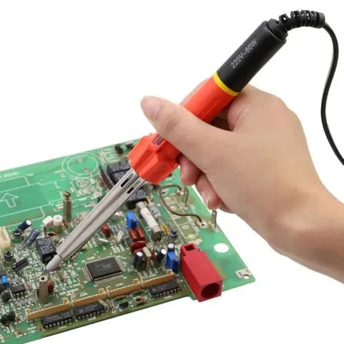
- Never use a charged soldering iron for welding. Confirm the iron is unpowered, and ideally ground its casing. Exercise extra caution with MOS circuits; using a 6–8V low-voltage soldering iron is safer.
- Understand Integrated Circuit (IC) and Circuit Principles
- Before inspecting or repairing integrated circuits, familiarize yourself with their functions, internal structures, key electrical parameters, pin functions, normal pin voltages/waveforms, and the working principles of peripheral circuits. This knowledge will greatly simplify analysis and troubleshooting.
- Avoid Pin Shortages During Testing
- When measuring voltage or testing waveforms with an oscilloscope probe, ensure the probe or test lead does not slip and cause short circuits between IC pins. It is best to measure on the peripheral printed circuit directly connected to the pins. Even momentary short circuits can easily damage ICs, especially when testing flat-packaged CMOS integrated circuits.
- Use High-Resistance Test Instruments
- When measuring DC voltage at IC pins, use a multimeter with a meter head internal resistance greater than 20KΩ/V to avoid significant measurement errors on certain pins.
- Ensure Heat Dissipation for Power Integrated Circuits
- Power integrated circuits must have adequate heat dissipation. Do not operate them at high power without a heat sink.
- Route Leads Reasonably
- If external components need to be added to replace damaged parts inside an IC, use small components and route wires reasonably to avoid unnecessary parasitic coupling, particularly when handling the grounding terminals between audio power amplifier ICs and preamplification circuits.
- Guarantee Welding Quality
- Ensure firm soldering to prevent dry joints caused by solder accumulation or air bubbles. Limit welding time to no more than 3 seconds, and use a 25W internal-heating soldering iron. After welding, carefully inspect the IC with an ohmmeter to confirm no short circuits between pins before powering up.
- Do Not Rush to Declare IC Failure
- Avoid prematurely concluding that an IC is faulty. Most ICs use direct coupling, so a malfunction in one circuit can cause voltage changes in multiple locations, which may not be due to IC damage. Additionally, normal or near-normal pin voltages do not always indicate a healthy IC, as some soft faults may not affect DC voltage readings.
02 PCB Debugging Methods
For a newly received PCB board, first conduct a visual inspection for obvious issues such as cracks, short circuits, or open circuits. If necessary, check the resistance between the power supply and ground to ensure it is sufficiently high.
Debugging a newly designed circuit board can be challenging, especially for large boards with many components. However, mastering a systematic debugging method can significantly improve efficiency.
Debugging a newly designed circuit board can be challenging, especially for large boards with many components. However, mastering a systematic debugging method can significantly improve efficiency.
PCB Debugging Steps:
- Initial Visual Inspection
- Visually check the new PCB for visible defects (e.g., cracks, short circuits, open circuits). Measure the resistance between the power supply and ground if needed.
- Stage-by-Stage Component Installation
- For independent modules, install components in phases rather than all at once (small circuits can be fully installed immediately). This helps narrow down fault locations.
- Start with the power supply module. Power up the board and test whether the output voltage is normal. When powering up, use a current-limited adjustable voltage source with a fuse as a precaution. Gradually increase the voltage while monitoring input current, input voltage, and output voltage. If no overcurrent occurs and the output voltage is normal, the power supply is functioning properly. If not, disconnect the power supply, locate the fault, and repeat the steps until the power supply is fixed.
- Incremental Module Installation and Testing
- Install other modules one by one, powering up and testing each module using the same voltage-ramping method to avoid component damage from design or installation errors.

- Install other modules one by one, powering up and testing each module using the same voltage-ramping method to avoid component damage from design or installation errors.
03 Methods for Locating PCB Faults
- Voltage Measurement Method
- First, verify that the voltage at the power pins of each chip is normal. Then check various reference voltages and operating voltages at other points. For example, a conducting silicon transistor typically has a BE junction voltage of about 0.7V and a CE junction voltage of 0.3V or lower. If a transistor’s BE junction voltage exceeds 0.7V (except for special transistors like Darlington tubes), the BE junction may be open.
- Signal Injection Method
- Apply a signal source to the input terminal and measure waveforms at subsequent points in sequence to identify faults. A simpler approach is to touch the input terminals of each stage with tweezers (note: avoid using this method on high-voltage or hot chassis circuits to prevent electric shock). If the post-stage reacts but the pre-stage does not, the fault likely lies in the pre-stage and should be prioritized for inspection.
- Other Fault Detection Methods
- There are many other ways to locate faults, such as visual, auditory, olfactory, and tactile inspections:
- Visual Inspection: Look for obvious physical damage to components, such as cracks, burn marks, or deformation.
- Auditory Inspection: Listen for abnormal operating sounds, such as unexpected noises or the absence of expected sounds.
- Olfactory Inspection: Check for unusual odors, such as burning or the smell of capacitor electrolyte. Experienced electronics repair technicians are highly sensitive to these odors.
- Tactile Inspection: Use your hand to test whether component temperatures are normal (e.g., excessively hot or cold).
- Power devices should generate heat during operation; if a component feels cool, it is likely not functioning. Conversely, overheating in non-power components or excessive heat in power components is also a problem. Generally, power transistors and voltage regulator chips can operate safely below 70°C. To gauge 70°C: if you can keep your hand on the component for more than 3 seconds, the temperature is below 70°C (exercise caution and test tentatively to avoid burns).
- There are many other ways to locate faults, such as visual, auditory, olfactory, and tactile inspections:
Related Posts
PCBA Prototype
December 14, 2025
PCB Assembly
September 2, 2025


