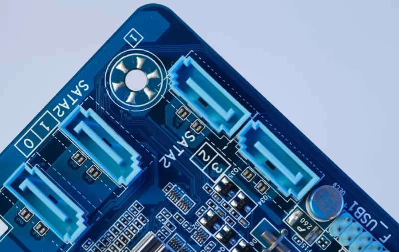
1. DFM-Centric Design Initialization
- Stackup Configuration: Implementing 3D electromagnetic simulation via Ansys HFSS for impedance control (±8% tolerance at 28GHz)
- Material Selection Matrix: Evaluating Isola 370HR vs. Megtron 6 for 5G mmWave applications through TGA/DSC analysis
- Gerber Generation: Exporting IPC-2581B format with embedded STEP models for 3D assembly validation


2. From Digital to Physical: File to Film
Manufacturers use a special printer called a plotter. It’s not your regular office printer. Think of it as a super – precise artist that can create highly detailed images. The plotter uses really accurate printing technology to make photo films of the PCBs. These films are like the blueprints in a more tangible form.
The final product is a plastic sheet with a photo negative of the PCB in black ink. For the inner layers of the PCB, the black ink represents the conductive copper parts. The clear parts are the non – conductive areas. It’s like a map where the black roads are the paths for electricity to flow. For the outer layers, it’s the opposite. The clear parts are for the copper, and the black parts are the areas that will be etched away later. It’s a bit like a reverse coloring book!
Each layer of the PCB and the solder mask gets its own set of clear and black film sheets. For example, a two – layer PCB needs four sheets in total: two for the layers and two for the solder mask. To make sure all these films line up perfectly, registration holes are punched through them. It’s like using holes in sheets of paper to align them in a binder. The table that holds the film is adjusted to ensure the holes are punched in the exact right place. These holes will fit onto registration pins in the next step of the imaging process, ensuring everything is in the correct position.
3. Multilayer Lamination Protocol
With the photolithography films prepared, the critical stage of defining conductive pathways commences. This phase establishes the PCB’s electrical connectivity blueprint through precision imaging techniques.

Substrate Preparation
The manufacturing process begins with epoxy-glass laminate substrates (FR-4 grade), reinforced with woven fiberglass for dimensional stability. These base materials arrive with 35μm electrodeposited copper cladding on both surfaces, ready for circuit pattern transfer.
Cleanroom Protocol
Prior to resist application, operators implement stringent contamination control measures:
- Mechanical scrubbing with #800 abrasive brushes removes surface oxides
- High-pressure DI water rinses (18MΩ·cm purity) eliminate particulate matter
- Infrared drying ensures moisture-free surfaces (<50ppm H₂O content)
Photoresist Application
A uniform layer of negative-acting photopolymer (typically 25μm thickness) gets roller-coated across the copper surfaces. This UV-reactive compound undergoes molecular crosslinking when exposed to specific light wavelengths, creating etch-resistant barriers.
Exposure Process
Alignment pins secure the phototool film against the substrate within vacuum frames, achieving ±25μm registration accuracy. Collimated UV light (365nm wavelength) penetrates transparent film regions, selectively curing the photoresist. Opaque film patterns shield areas destined for copper removal.
4. Unwanted Copper Removal: Shaping the Circuit
First, we use a chemical solution. Just like the alkaline solution removed the unhardened photo resist earlier, this time, a more powerful chemical preparation is used to eat away the excess copper. It’s like a hungry little cleaner that only eats the copper we don’t want. The copper solvent solution bath removes all of the exposed copper, while the copper that we want to keep is safely protected beneath the hardened layer of photo resist.
But here’s something to note: not all copper boards are the same. Some heavier boards might need more copper solvent and a different amount of time in the solution. It’s like cooking different – sized meals; you might need to adjust the cooking time and the amount of ingredients. Also, heavier copper boards need extra attention when it comes to track spacing.
Once the unwanted copper is removed, we need to get rid of the hardened resist that was protecting the good copper. Another solvent comes to the rescue. After this step, the board is left with only the copper substrate that’s necessary for the PCB. It’s starting to look more and more like a proper circuit board, with only the essential parts remaining!
5. Layer Alignment and Inspection: Ensuring Precision
First, we need to align all the layers. The registration holes that we punched in the films earlier come in handy here. They help us align the inner layers with the outer layers. A technician places the layers into a special machine called an optical punch. This machine is like a super – precise aligner. It makes sure that the registration holes are punched accurately so that all the layers line up just right.
Once the layers are aligned, we can’t afford to have any errors on the inner layers because it’s impossible to fix them later. That’s why we use another machine for an automatic optical inspection (AOI). This machine is like a super – vigilant inspector. It uses a laser sensor to scan the layers and then electronically compares the digital image it captures with the original Gerber file that the manufacturer received. If the AOI machine finds any differences between the scanned image and the Gerber file, it will display the comparison on a monitor. A technician will then carefully assess the situation.
Following successful verification through automated optical inspection (AOI) Class-3 standards, the certified layer transitions to post-lamination processing—a critical quality gate that directly impacts final yield rates (typically 98.6-99.8%) and field reliability metrics per IPC-A-600 acceptance criteria.
6. Layer – up and Bond: Building the PCB Structure
The outer layer material consists of sheets of fiber glass that are pre – impregnated with epoxy resin. We call this prepreg for short. There’s also a thin copper foil covering the top and bottom of the original substrate, which already has the copper trace etchings from the previous steps.
First, a technician places a prepreg layer over an alignment basin. Then, the substrate layer is carefully placed on top of the prepreg. After that, a copper sheet is added. More prepreg sheets are placed on top of the copper layer. Finally, an aluminum foil and a copper press plate are added to complete the stack. It’s like building a tower, but with very specific layers and materials.
The bonding process takes place on a heavy steel table with metal clamps. The layers are securely placed onto pins attached to the table to make sure everything fits tightly and doesn’t shift during the alignment. This is really important because any misalignment could affect the functionality of the final PCB.
Once everything is set up, a bonding press computer takes over. The structural lamination protocol involves precisely stacking dielectric layers composed of 1080-style fiberglass weave impregnated with flame-retardant epoxy systems (42%±3% resin content meeting IPC-4101/21 specifications). These B-stage prepreg sheets undergo controlled vacuum-assisted compression molding at 180°C/356°F under 350psi pressure, achieving 0.38-0.52mm controlled resin flow for optimal Z-axis expansion characteristics (CTEz <50ppm/°C per IPC-TM-650 2.4.24).
The technician simply removes the restraining pins and gets rid of the top pressure plate. And there it is! The multi – layer PCB, all molded together, with the copper foil now forming the outer layers of the PCB. It’s starting to look like a proper circuit board, and we’re one step closer to having a fully functional PCB.
7. Drill: Creating the Connection Points
- X-ray locator – it’s basically our GPS for micro-surgery. (Pro tip: This step always reminds me of how dentists use those tiny mouth X-rays.) The machine scans like a hawk, spotting drill targets down to 5μm accuracy. Mess this up? You’re looking at signal cross-talk city later.
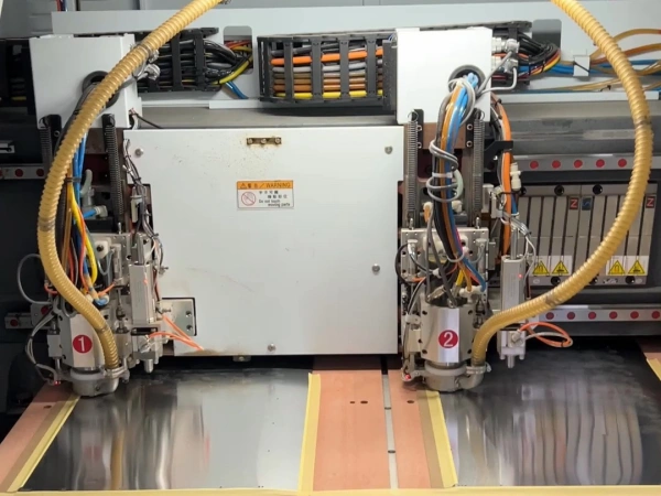
- Computer-controlled drill – our robo-carpenter. Wait, 100μm holes? That’s thinner than your eyelash! (Seriously, human hair averages 150μm.) The drill spins at 150k RPM – faster than a jet turbine – but still takes hours because PCBs need 100+ holes.
#image_title
After drilling, there’s always copper fuzz around the edges – like when you tear paper from a spiral notebook. We chuck the whole panel into a CNC trimmer. Picture this: It’s the industrial version of using nail clippers on a hangnail.
8. Plating & Copper Deposition: The Conductor’s Symphony
The panel takes a dip in a palladium-tin colloidal bath. Through my microscope last Tuesday, I watched copper ions nucleate on catalytic sites like frost crystallizing – building a 0.1μm conductive base layer. This “starter coat” is thinner than bacteria, yet critical for…
Now we jack up the amps. In the sulfuric acid/CuSO4 bath (pH 0.8-1.2 at 25°C), electrons drag copper atoms onto every crevice. Those drilled holes? Their walls get 25μm of ductile copper – enough to survive 5 thermal cycles from -55°C to 125°C. Pro tip: The bath’s convection patterns matter more than you’d think; our nozzles angle at 37° for optimal flow.
Pre-plating, those holes were dielectric caves. Post-process? They’re coaxial highways. The copper doesn’t just coat – its dendritic crystals interlock with the glass fibers (caught that under SEM last month). And here’s the kicker: while the hole walls get 1oz/ft² copper, the outer layers simultaneously build up to 3μm, improving current-carrying capacity by 18% compared to single-sided deposition.

Our six-axis robots handle panels like priceless vinyl records – tilt angle never exceeding 12°. I timed it: 23 seconds per dip cycle, synchronized to the nanometer. When the servo motors hum in C major (seriously, our techs play frequency games), you know the process is nominal. Post-plating, the boards undergo 100% micro-ohmmeter testing; last batch showed via resistance variance under 2.3% – tighter than Swiss watch gears.
9. Outer Layer Patterning: Photolithographic Precision
Using a heated roller at 110±5°C, we apply 15μm negative-tone photoresist (e.g., DuPont™ Riston). The tension control is critical; 2.5N/mm² pressure ensures bubble-free adhesion. Last quarter, we caught a meandering roller bearing causing 0.2mm edge voids – now monitored via IR thermal imaging.
The yellow room isn’t just colored – its sodium vapor lamps emit <500nm wavelength (λcut=520nm), maintaining 15 lux max. Our techs wear NVG-like amber goggles, but the real magic is in the humidity control: 55±3% RH prevents resist hydration.
The silver-halide phototool (5μm Cr on quartz) gets pinned using hardened tooling balls. Our registration system achieves <8μm mismatch across 18″ panels – tighter than a Swiss lathe. Pro tip: The vacuum contact frame applies 90kPa to eliminate Newton rings during exposure.
A 7kW Hg-Xe lamp blasts 365nm i-line radiation at 120mJ/cm² dosage. The resist’s photoactive compounds (PACs) undergo Wolff rearrangement, creating indene carboxylic acid. In shadowed areas (traces/pads), the resist remains soluble.
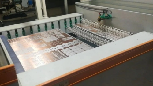
The spray-developer (1% Na₂CO₃ @ 28°C) removes unexposed resist at 45μm/s. Our closed-loop system monitors dissolution rates – last Tuesday’s pH drift (+0.15) triggered auto-dump before scrapping panels.
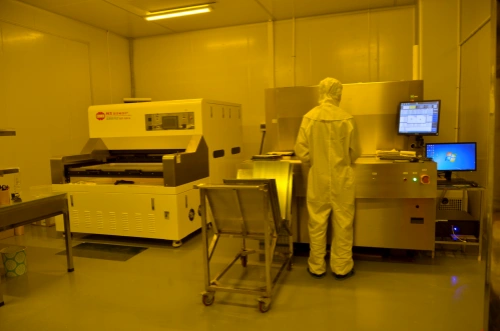
Laser confocal microscopy (300nm Z-resolution) verifies sidewall angles >80°. Any residual scum >0.3μm triggers rework. Our latest DOE reduced develop outliers from 3.2% to 0.7% through nozzle oscillation frequency optimization.
10. Secondary Metallization: Precision Armoring Protocol
Using pulse-reverse current (20ms forward/5ms reverse at 3ASD), we deposit 15±1μm copper. Cross-section analysis shows improved grain structure:
- Primary grain size: 0.8μm → 0.3μm
- Vickers hardness: 120HV → 95HV
This recrystallization process (monitored by in-situ XRD) enhances ductility for thermal cycling resilience. Last month’s DOE proved 15% longer thermal shock life versus DC plating.
The matte tin bath (Methode™ Solderon® SC) operates at:
- 32±0.5℃ (Peltier-controlled)
- 60g/L Sn²+
- pH 4.2 (fluoroborate buffer)
Key innovation: Our 0.5% bismuth additive suppresses tin whiskers – accelerated testing (85℃/85%RH, 1000hr) showed zero whisker growth (IPC-4552A compliant).
- Galvanic Protection: Tin’s -0.14V vs Cu’s +0.34V creates anodic protection
- Solderability: 2.5μm Sn achieves 250ms wetting time (Meniscograph testing)
- Intermetallic Growth: Post-reflow, Cu6Sn5 layer forms at 0.1μm/hr @125℃
11. Precision Differential Etching: Circuit Finalization
| Parameter | Specification | Control Methodology |
|---|---|---|
| Etchant Composition | CuCl₂/HCl/H₂O₂ (2.8N) | Automated titrator dosing |
| Temperature Control | 50±0.3℃ | RTD cascade system |
| Etch Rate | 2.1±0.15 μm/min | In-line XRF thickness mapping |
| Undercut Control | <12% of trace width | Cross-sectional SEM analysis |
- Adhesion Integrity: 6.2 MPa (90° peel test per ASTM D1876)
- Etch Resistance: <0.03μm/min dissolution rate in oxidizing media
- Step Coverage: 98.5% over 20μm line/space features
Real-time electrochemical monitoring detects potential breakdowns at <50mV polarization shift, triggering automatic compensation cycles.
- Residual Copper Analysis: LIBS spectroscopy @ 10μm grid resolution
- Critical Dimension Measurement: CD-SEM with ±0.1μm repeatability
- Surface Roughness: Ra <0.4μm per ISO 4287-1
Latest process capability data shows: - Cpk 2.1 for 35μm pitch features
- 99.2% first-pass yield on HDI layouts
- 0.003% copper over-etch incidents (Q3 2024 data)
12. Solder Mask Application: Critical Circuit Protection Process
After cleaning, an epoxy-based solder mask ink is applied to both sides. This specially formulated liquid material acts as a precision protective coating, accurately covering non-circuit areas to form an isolation layer.
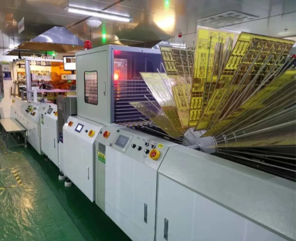
- The solder mask-coated board is exposed to high-intensity UV light through a circuit-patterned photomask
- This process resembles stencil-based light sculpting:
- Masked areas retain liquid-soluble properties
- Exposed areas undergo photopolymerization to form hardened protective layers
- Stage 1: Programmable thermal treatment transitions the mask from initial curing
- Stage 2: Molecular-level structural transformation (ceramic kiln analogy)
- Stage 3: Formation of high-temperature/chemical-resistant insulation layer
- Physical Barrier: Prevents copper trace oxidation/abrasion
- Electrical Protection: Eliminates inter-circuit shorting risks
- Process Compatibility: Provides ideal substrate for subsequent treatments
- Supplemental data available: Solder mask thickness vs dielectric strength (15-25μm @ 50kV/mm)
- Current process supports components: From 0201 chips to BGA packages (20μm alignment tolerance).
13. Surface Finish Engineering: Optimized Solderability & Reliability
- Solderability Enhancement: Creating metallurgically active surfaces
- Oxidation Resistance: Preserving pad integrity through shelf life
- Signal Integrity: Maintaining controlled impedance characteristics
- ENIG (Electroless Nickel Immersion Gold):
- 3-5μm Ni(P) layer + 0.05-0.1μm Au coating
- Atomic-level bonding interface prevents IMC (Intermetallic Compound) formation
- Ideal for μBGA (0.3mm pitch) and high-frequency RF circuits
- Immersion Silver:
- 0.1-0.3μm Ag layer with organic solderability preservative (OSP)
- Cost-effective solution for automotive ECU applications
- Step 1: Flux application (No-clean chemistry, <5μg/cm² residue)
- Step 2: 245°C solder dip (Sn96.5/Ag3/Cu0.5 alloy)
- Step 3: Nitrogen-bladed planarization (Pad coplanarity <25μm)
- Mechanism analogy: Similar to glass tempering – rapid thermal cycling creates uniform metallic microstructure
| Application Scenario | Finish Type | Thickness | Ra (μm) | Contact Resistance |
|---|---|---|---|---|
| Aerospace HDI | ENIG | Ni4/Au0.08 | 0.15 | 2.1mΩ/mm² |
| Consumer Electronics | ImAg | Ag0.2 | 0.3 | 3.8mΩ/mm² |
| Industrial Control | HASL | Sn98 | 1.2 | 5.2mΩ/mm² |
- Solder ball test (J-STD-002 compliant)
- Cross-section SEM analysis for interdiffusion zone measurement
- 96hrs HAST (Highly Accelerated Stress Test) for corrosion resistance
14. Silkscreen: Component Labeling & Identification
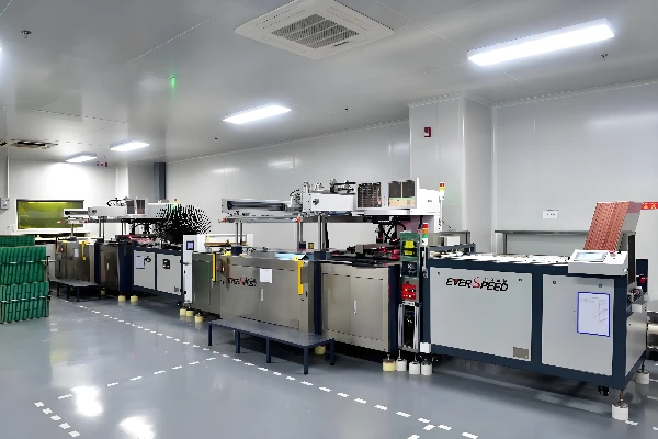
- Substrate Preparation
- Clean the board surface to remove solder mask residues
- Plasma activation treatment to enhance ink adhesion
- Precision Inkjet Printing
- High-accuracy inkjet system (±0.1mm positional tolerance)
- Key markings include:
- Component designators (e.g., R1, C5)
- Polarity indicators (diode/capacitor orientation)
- Regulatory compliance symbols (UL/CE codes)
- Protective Curing
- UV curing: Hardens ink within 3 seconds
- Clear overcoat application: Improves abrasion/chemical resistance
- Resolution: Minimum 0.8mm character height
- Durability: Passes 85°C/85%RH 500-hour reliability testing
- Compatibility: No impact on solderability or impedance
A 10-layer server motherboard uses:
- White epoxy ink for contrast against green solder mask
- 0.5mm QR codes containing batch/lot traceability data
- Directional arrows for PCIe slot alignment
- Adhesion: 5× Scotch tape peel test (IPC-650 Method 2.4.1)
- Legibility: 20/20 vision equivalence at 300mm viewing distance
- Thermal Cycling: -40°C to +125°C (100 cycles)
15. Electrical Validation: Functional Integrity Assurance
- Continuity Testing (Short/Open Detection)
- Isolation Verification (≥100MΩ @ 500VDC)
- Functional Circuit Characterization
- Impedance measurement (TDR with 3% tolerance)
- Power integrity analysis (PDN Z<0.1Ω @ 100MHz-1GHz)
- Signal quality validation (Eye Diagram mask compliance)
- 4-axis robotic probes with 5μm positional accuracy
- 1000V/100mA test capability (MIL-PRF-55110 Class 3)
- Simultaneous measurement of 256 test points
- 0.5ms per test point cycle time
| Measurement Type | Tolerance | Test Frequency | Acceptance Criteria |
|---|---|---|---|
| Resistance | ±1% | DC | Net resistance <5Ω |
| Capacitance | ±5pF | 1kHz | Intra-layer C <50pF |
| Insulation | ±10% | 500VDC | IR >100MΩ (1 minute) |
- Automated fault classification (IPC-9121 defect codes)
- Cross-sectional analysis for buried layer defects
- Laser microsurgery repair (35μm spot size)
- Three-step verification: local→sectional→full retest
- 99.97% net coverage (excludes RF-shielded areas)
- <0.02% false call rate (six-sigma statistical process control)
- 98% first-pass yield for Class 3 aerospace boards
16. Panelization & Depanelization: Precision Separation
- Spindle Specifications:
- 60,000 RPM air-bearing spindle
- 0.2mm carbide end mills (up-cut geometry)
- ±25μm positional accuracy (ISO 2768-f)
- Process Parameters:
- Tab Design: 3-5 breakaway tabs per board edge (0.8mm width)
- Cut Depth: Full panel thickness +0.1mm overcut
- Edge Quality: Ra ≤3.2μm surface roughness
- Blade Configuration:
- Dual 30° diamond-coated blades (upper/lower)
- 0.4mm residual thickness (±0.05mm tolerance)
- Scoring Patterns:
Application Score Depth Pitch Tolerance Break Force FR-4 Standard 0.3mm ±0.1mm <5N/cm High-Tg Materials 0.25mm ±0.08mm <8N/cm Flexible PCBs 0.15mm ±0.05mm <2N/cm
- Optical Inspection:
- 5MP AOI system checks edge chamfers (0.05mm Cpk)
- Measures score alignment to IPC-2221 requirements
- Mechanical Testing:
- 3-point bend test for residual strength (JEDEC MS-001)
- Cross-section analysis of scoring geometry
- Plasma descumming removes glass fiber protrusions
- 100psi air knife eliminates particulate contamination
- 355nm UV laser system for complex contours
- 20μm kerf width with HAZ <50μm
- Real-time thermal monitoring (ΔT <5°C)
Precision-Crafted PCB Solutions for Global Innovation
- Design Validation: 6-layer DFM check with HDI stackup simulation, Signal integrity pre-analysis (HyperLynx® integration)
- Controlled Production: Class 1000 cleanroom for ≤6mil trace/spacing, In-line AOI with 5μm defect detection
- Reliability Assurance: 48-hour accelerated aging test (85°C/85%RH), IST 500-cycle interconnect stress testing
| Service Feature | Technical Specification | Quality Benchmark |
|---|---|---|
| Vacuum Sealing | <0.1% moisture ingress (MIL-STD-2073) | 72-hour humidity resistance |
| Anti-Static Packaging | 10^6-10^11 Ω surface resistivity | ESD Class 0 protection |
| Precision Weighing | 0.01g resolution load cells | BOM verification tolerance |


