The Design of Multi – layer PCBs: Eight Steps
By PCBA PrototypePublished On: 2025-05-06Categories: Uncategorized0 Comments on The Design of Multi – layer PCBs: Eight Steps
By PCBA PrototypePublished On: 2025-05-06Categories: Uncategorized0 Comments on The Design of Multi – layer PCBs: Eight Steps
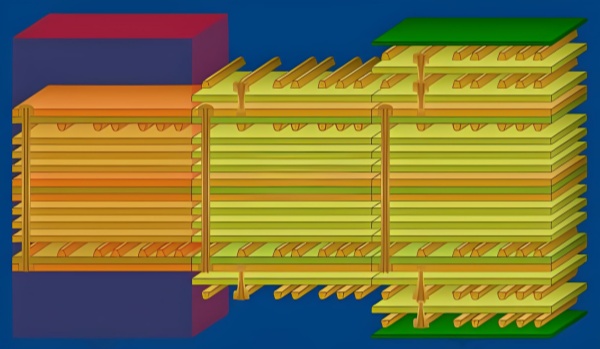
A multi – layer PCB is a special type of printed circuit board. Its location is usually quite special. For example, multi – layer PCBs can be found in circuit boards. This kind of multi – layer board can help the machine connect various different circuits. Moreover, it can also play an insulating role, preventing electricity from interfering with each other and ensuring absolute safety. If you want to use a multi – layer PCB with relatively good performance, careful design is essential. Next, we will explain how to design a multi – layer PCB.
PCB Multi – layer Board Design:
1. Determination of Board Shape, Size, and Number of Layers
For any printed circuit board, there is an issue of matching and assembling with other structural components. Therefore, the shape and size of the printed circuit board must be based on the overall structure of the product. However, from the perspective of production technology, it should be as simple as possible. Generally, it is a rectangle with a not – too – large aspect ratio, which is conducive to assembly, improving production efficiency, and reducing labor costs.

Regarding the number of layers, it must be determined according to the requirements of circuit performance, board size, and the density of the circuit lines. For multi – layer printed circuit boards, four – layer and six – layer boards are most widely used. Take a four – layer board as an example, which consists of two conductor layers (component side and soldering side), one power layer, and one ground layer.
Each layer of a multi – layer board should be symmetrical, and it is best to have an even number of copper layers, such as four, six, or eight layers. Because asymmetric lamination is likely to cause warping of the board surface, especially for surface – mounted multi – layer boards, this should be paid more attention to.
2. Location and Placement Direction of Components
The location and placement direction of components should first be considered from the perspective of circuit principles, conforming to the direction of the circuit. Whether the placement is reasonable or not will directly affect the performance of the printed circuit board. Especially for high – frequency analog circuits, the requirements for the location and placement of components are even more stringent.
Reasonable placement of components, in a sense, already indicates the success of the printed circuit board design. Therefore, when starting to arrange the layout of the printed circuit board and determine the overall layout, a detailed analysis of the circuit principle should be carried out. First, determine the location of special components (such as large – scale ICs, high – power transistors, signal sources, etc.), and then arrange other components, trying to avoid factors that may cause interference.

On the other hand, from the perspective of the overall structure of the printed circuit board, the uneven and disorderly arrangement of components should be avoided. This not only affects the appearance of the printed circuit board but also brings a lot of inconvenience to assembly and maintenance work.
3. Requirements for Conductor Layers and Wiring Areas
Generally, the wiring of multi – layer printed circuit boards is carried out according to circuit functions. When wiring on the outer layers, it is required to have more wiring on the soldering side and less wiring on the component side, which is conducive to the maintenance and troubleshooting of the printed circuit board. Thin, dense conductors and signal lines vulnerable to interference are usually arranged on the inner layers. Large – area copper foils should be distributed relatively evenly on the inner and outer layers. This will help reduce the warping degree of the board and also enable a more uniform coating to be obtained on the surface during electroplating. To prevent the printed conductors from being damaged during shape processing and to avoid inter – layer short – circuits during machining, the distance between the conductive patterns in the inner and outer layer wiring areas and the edge of the board should be greater than 50 mil.
4. Requirements for Conductor Direction and Width
The routing of multi – layer boards should separate the power layer, ground layer, and signal layer to reduce interference between power, ground, and signals. The lines on adjacent layers of the printed circuit board should be as perpendicular to each other as possible, or take diagonal or curved paths, and should not be parallel, to reduce inter – layer coupling and interference of the substrate. And conductors should take the shortest paths as much as possible. Especially for small – signal circuits, the shorter the line, the smaller the resistance and the less the interference. When changing direction, the signal lines on the same layer should avoid sharp – angled turns. The width of the conductors should be determined according to the requirements of the circuit for current and impedance. The power input lines should be wider, and the signal lines can be relatively narrower. For general digital boards, the width of the power input lines can be 50 – 80 mil, and the width of the signal lines can be 6 – 10 mil.
Conductor width: 0.5, 1, 0, 1.5, 2.0;
Allowable current: 0.8, 2.0, 2.5, 1.9;
Conductor resistance: 0.7, 0.41, 0.31, 0.25;
Allowable current: 0.8, 2.0, 2.5, 1.9;
Conductor resistance: 0.7, 0.41, 0.31, 0.25;
When routing, attention should also be paid to keeping the width of the lines as consistent as possible, avoiding sudden thickening or thinning of the conductors, which is beneficial to impedance matching.
5. Requirements for Drill Hole Size and Pad
The size of the component drill holes on a multi – layer board is related to the size of the component lead pins. If the drill hole is too small, it will affect the insertion of the component and soldering; if the drill hole is too large, the solder joint will not be full enough during soldering. Generally, the calculation methods for the diameter of the component hole and the pad size are as follows:
Component hole diameter = component lead pin diameter (or diagonal) + (10 – 30 mil)
Component pad diameter ≥ component hole diameter + 18 mil
Component pad diameter ≥ component hole diameter + 18 mil
As for the via hole diameter, it is mainly determined by the thickness of the finished board. For high – density multi – layer boards, it is generally necessary to control it within the range of board thickness : via hole diameter ≤ 5 : 1. The calculation method for the via hole pad is:
Via hole pad (VIAPAD) diameter ≥ via hole diameter + 12 mil
6. Requirements for Power Layer, Ground Layer Partitioning and Flower – shaped Holes
For multi – layer printed circuit boards, there is at least one power layer and one ground layer. Since all voltages on the printed circuit board are connected to the same power layer, the power layer must be partitioned and isolated. The size of the partition line is generally 20 – 80 mil in width. The higher the voltage, the thicker the partition line.
At the connection between the solder holes and the power layer and ground layer, to increase reliability and reduce the occurrence of false soldering caused by large – area metal heat absorption during soldering, the connection pads are generally designed in a flower – shaped hole shape.
Isolated pad diameter ≥ drill hole diameter + 20 mil
7. Requirements for Safety Clearance
The setting of the safety clearance should meet the requirements of electrical safety. Generally, the minimum clearance of the outer layer conductors should not be less than 4 mil, and the minimum clearance of the inner layer conductors should not be less than 4 mil. When the wiring allows, the clearance should be as large as possible to improve the yield rate during board manufacturing and reduce potential faults of the finished board.
8. Requirements for Improving the Anti – interference Ability of the Entire Board
In the design of multi – layer printed circuit boards, attention must also be paid to the anti – interference ability of the entire board. Common methods include:
a. Add filter capacitors near the power and ground of each IC, with a capacity generally of 473 or 104.
b. For sensitive signals on the printed circuit board, add accompanying shielding lines respectively, and try to have as little wiring as possible near the signal source.
c. Select a reasonable grounding point.

You must have understood the design method of multi – layer PCBs. However, you may not know what the parameters of this kind of multi – layer board are. The minimum aperture of a multi – layer PCB is generally 0.4mm, which is a necessary design. When designing a multi – layer PCB, we must adjust its thickness and size to a range suitable for electrical appliances. Neither too large nor too small is appropriate. When performing surface treatment, the electro – gold – plating method must be selected; otherwise, the insulating property may be lost.
Related Posts
PCBA Prototype
December 14, 2025
PCB Assembly
September 2, 2025


