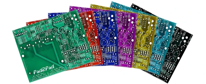
Structure and Connection Methods in Electronic Manufacturing Tags

In the electronic manufacturing field, PCBA (Printed Circuit Board Assembly) is a crucial step that involves the assembly and processing of circuit boards. For procurement personnel in electronic device manufacturers, understanding the structure and connection methods of PCBA circuit boards is essential. This knowledge not only relates to product quality but also directly impacts production efficiency and cost control.
1. Structure of PCBA Circuit Boards
Substrate:
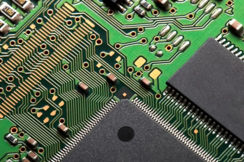
The substrate is the foundation of the PCBA circuit board, typically made from insulating materials such as fiberglass, polyimide, or other synthetic materials. The thickness, material, and surface treatment process of the substrate have a significant impact on the performance and reliability of the circuit board.
Conductive Layer:
The conductive layer is the part of the circuit board that conducts electricity, usually made of copper foil, formed into specific circuit patterns through chemical etching or mechanical cutting. The thickness, width, and spacing of the conductive layer affect the efficiency and stability of current transmission.
Components:
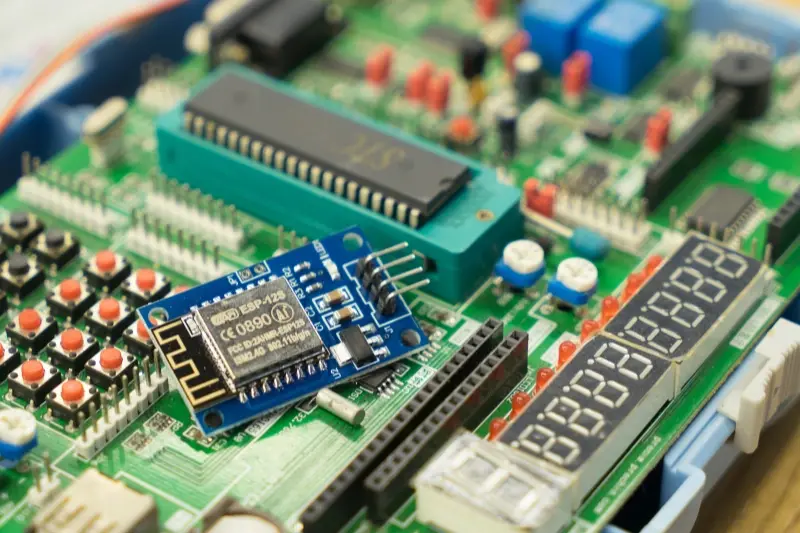
The components on the PCBA circuit board include resistors, capacitors, inductors, IC chips, etc. These components are fixed to the circuit board through soldering or other connection methods and are interconnected through the conductive layer.
Pads and Vias:
Pads are the locations where the component leads connect to the conductive layer, typically designed as circular or square metal pieces. Vias are metallized passages that connect different conductive layers, ensuring smooth current flow between multi-layer circuit boards.
Solder Mask and Silkscreen Layer: The solder mask protects the conductive layer, preventing unnecessary electrical connections and short circuits. The silkscreen layer is used to mark the positions, numbers, and other important information of the components, facilitating production and maintenance.
2. Connection Methods for PCBA Circuit Boards
Soldering:
Soldering is the most common connection method, which involves melting solder to connect the component leads with the pads on the circuit board. Depending on process requirements, methods such as wave soldering, reflow soldering, or hand soldering can be selected.
Plugging:
The plugging method is suitable for larger components or connectors, achieving electrical connections through mechanical connections of pins and sockets. This method facilitates the replacement and maintenance of components, although its connection stability may be slightly inferior to soldering.
Crimping:
Crimping connects the component leads by pressing them into the holes on the circuit board. This method is suitable for high-frequency and high-current connections, offering lower resistance and inductance.
Conductive Adhesive Bonding:
Conductive adhesive is a bonding agent with conductive properties that can attach components to the circuit board and establish electrical connections. This method is suitable for temperature-sensitive components, avoiding the high temperatures associated with soldering.
Screw Fixation:
For larger or heavier components, screw fixation can be used to ensure connection stability and reliability. This method requires pre-drilled installation holes on the circuit board, along with appropriate nuts or bolts.
Understanding the structure and connection methods of PCBA circuit boards is crucial for procurement personnel in electronic device manufacturers. This knowledge not only helps in selecting high-quality circuit board suppliers but also aids in avoiding potential problems and risks during product design and production.
By gaining a deeper understanding of these fundamental concepts, procurement personnel can make more informed decisions, ensuring that the performance and reliability of electronic products reach the highest levels.
Table of Contents
Tags
Related Posts
PCBA Prototype
January 25, 2026
PCBA Prototype
December 8, 2025
PCBA Prototype
April 6, 2025


