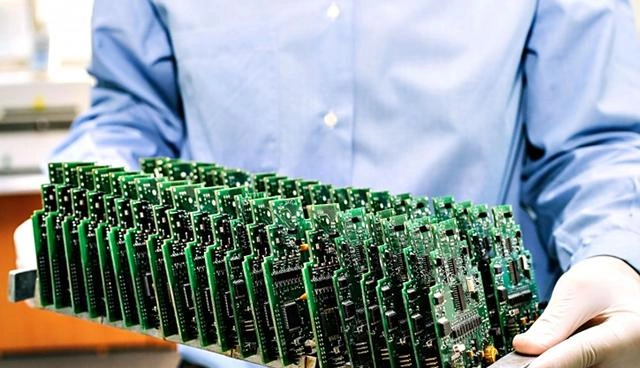
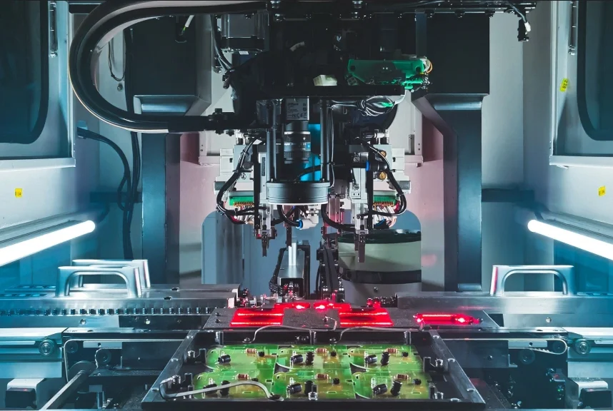
Plasma Cleaning Technology in PCB Manufacturing: Applications and Benefits

Plasma not only effectively removes organic contaminants on the surface of polymer materials, but it is also used for fine cleaning of organic contaminants on the surfaces of PCBA and PCB, ceramic panels, glass panels, metal panels, and other materials. It can remove surface pollutants, improve surface energy, and modify surfaces, thus enhancing bonding or adhesion processes in subsequent stages. Below, we will explore some application cases of plasma cleaning machines in PCB manufacturing processes.
In PCB manufacturing, plasma cleaning has distinct advantages over wet cleaning methods. For high-density multi-layer boards (HDI), micro-holes, multi-layer FPC desmear, rigid-flex PC desmear, and FR-4 high aspect ratio (width-to-length) micro-hole desmear (Desmear), plasma cleaning provides more thorough and effective results. Plasma cleaning is more stable and complete compared to chemical desmear processes, leading to a yield improvement of over 20%.
Cleaning Objectives:
- Thoroughly remove smear, accurately control etching results, improve the bonding strength of hole walls and copper plating, and increase hole plating reliability and yield. Prevent issues like uneven or defective PTH (Plated Through Hole) plating that could cause open circuits.
- Desmear for multi-layer flexible boards: Remove epoxy resin glue (Epoxy), acrylic glue (Acrylic), and other adhesives.
WireBonding Contaminants:
- Solder mask, residual glue, SMT residues, rosin, organic acids; decane (SMT cleaning solution residues) with major components like Polystyrene and Mylar (polyester film); metal oxide; hardened photosensitive elements like solder; organic and inorganic particles in the air, and residual liquids on the substrate. Plasma cleaning has limitations and is ineffective in removing some of these. However, plasma cleaning is highly effective in removing dry films and residues from fine hardware components and processing high-frequency boards, as shown in Figures 3 and 4.
Principle: Ar+e → Ar++2e → Ar++CxHy
After cleaning, the substrate can be monitored by measuring the pull force post-wire bonding, before molding, to assess the cleaning effectiveness. The primary purpose is to activate the substrate, increase the contact area, and enhance the physical activation of surface molecules, aiding in the bonding of molding compounds to the substrate.
Applications in Industries: Plasma cleaning can be applied in the microelectronics industry, optoelectronics industry, printed circuit industry, poor die attachment, poor wire bond strength, and flip-chip underfill, etc.
High Aspect Ratio FR-4 Hardboard Micro-Hole Desmear:
- Chemical cleaning agents often fail to penetrate into micro-holes due to surface tension, making the desmear process incomplete. Plasma cleaning, however, does not have this limitation and is especially effective for small apertures.
- Rigid-Flex PC Through-Hole Desmear: Plasma cleaning ensures complete desmear, avoids the chemical attack of potassium permanganate on flexible board PI, and improves the uniformity of the hole wall etching, enhancing copper plating reliability and yield.
Laser Processing Post-Cleaning of Charred Residues:
- HDI board laser through-holes, blind/embedded holes, and removal of laser-charred residues. Plasma cleaning is effective even for micro-via holes smaller than 50 microns.
Surface Roughening and Activation, Enhancing Adhesion:
- For rigid-flex boards, multi-layer high-frequency boards, and multi-layer mixed boards, plasma treatment can roughen the surface of materials such as PI or PTFE before lamination. This improves the bonding strength significantly, preventing delamination and ensuring stronger adhesion.
- FPC reinforcement pre-treatment: Plasma roughening of PI surfaces before reinforcing with steel sheets, aluminum sheets, or FR-4 can improve tensile strength by more than ten times, preventing material detachment.
Cleaning before Chemical Gold Plating / Electroplating Gold:
- Removal of solder mask ink and other foreign materials before gold finger and solder pad surface cleaning. Plasma cleaning improves wettability and prevents defects like soldering issues and poor tinning, enhancing reliability.
PTFE (Polytetrafluoroethylene):
- PTFE, commonly known as Teflon, is used for high-frequency circuit boards due to its excellent electrical properties.
High-Frequency Microwave Board Copper Plating Activation before Hole Surface Modification:
- Improves the bond strength between the hole wall and copper layer, preventing issues like black holes after copper plating, and eliminating high-temperature fractures of hole copper and inner layer copper, improving reliability.
Surface Activation before Solder Mask and Silkscreen:
- Prevents solder mask and silkscreen character detachment, ensuring better adhesion.
In precision mechanical and electronic manufacturing, traditional wet cleaning processes are increasingly limited, and research into dry cleaning mechanisms and applications is becoming urgent. Plasma cleaning technology shows clear advantages in dry cleaning applications, as it does not pose potential harm to the workpieces. Currently, plasma cleaning is widely applied in PCB manufacturing processes.