PCBA SMT Guide: Efficiency, Costs & Supplier Selection
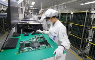
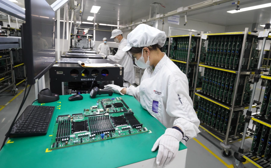
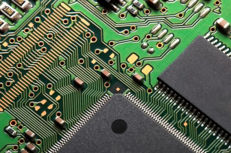
1. SMT Processing Efficiency For large-scale PCB production, the overall efficiency of an SMT manufacturing facility is very important. Regardless of whether a PCBA is high-precision or standard, the [...]

