PCB Stackup: Structure Shapes EMC
Electromagnetic Compatibility (EMC) is an important measure. It shows if electronic devices work well in an electromagnetic environment and do not cause problems for other devices. In PCB design, not handling EMC issues right can cause signal interference, system failure, or not meeting industry standards.
EMC problems usually come from current loops, signal return paths, and the spread of electromagnetic fields. In PCB design, the stack-up structure gives support and helps control electromagnetic interference (EMI). A good stack-up can lower radiation, block crosstalk, and keep signals strong. This article shows how to improve EMC performance by choosing layers, ordering them, and designing planes from a stack-up view.
1. Choosing the Number of Power and Ground Planes
For a PCB with one power supply, one power plane is enough. For many power supplies that do not overlap, you can use a separate power layer so that important signal traces on nearby layers do not cross split areas. But if power supplies overlap, use two or more power planes. You must do these things:
Each power plane has one power supply or several that do not overlap.
Important signal traces on nearby layers do not cross split areas.
Also, when choosing a ground plane, you must consider:
The layer under the component layer should have a full ground plane. If this is not possible in a multi-layer HDI board, small local ground planes are allowed.
High-frequency, RF, high-speed, and clock signals need a ground plane next to them.
Each power plane should have a ground plane next to it (for example, both layers next to a power plane should be ground layers).
More ground layers usually mean better EMC shielding, but more layers cost more money. A 4-layer board is a basic choice for EMC, with one power and one ground layer. A 6-layer board or more works for high-speed and high-density designs that need better shielding and reference planes. A 2-layer PCB is cheap but has weak EMC performance and depends on large ground areas.
In cost-sensitive consumer electronics, using fewer layers lowers cost. For example, when a product matures, cost-cutting may reduce layers, like changing a 10-layer board to an 8-layer one. In these cases, which layer should be removed: the ground layer or the power layer? Usually, PCB makers keep the ground plane better than the power plane. This is why smartphone PCBs do not have a separate power layer. They use the power layer for other signals, so it becomes a mix.
2. Choosing the Number of Signal Layers
When you import the netlist into PCB design software, it shows the number of components, pads, signal traces, and routing density. This helps to guess how many signal layers are needed. Skilled PCB designers adjust this guess by looking at the board’s operating frequency, the number of important signals with special routing needs, and cost versus performance.
Signal layers are given based on signal importance and direction. If you are not sure if there are enough layers, you can pre-route important signals on each layer to see if layers cross and if ground shielding works.
For mobile devices, think about signal layers like this:
Clock (CLK) traces need a ground (GND) shield on the sides.
RF (radio frequency) traces should go on the outer layers. If they go inside, they need ground planes next to them. 4G designs usually use one inner layer for RF. 5G and 6G may need 3 to 4 layers.
High-speed signals like IQ, USB, MIPI, HDMI, and LVDS need shielding and isolation. They should have their own layers. If they cross layers, ground planes next to them must shield them.
The number of signal layers is mainly set by what the board does. For EMC, use shielding or isolation on important signal networks (both those that radiate and those that are sensitive to noise).
3. Layout of Ground and Power Planes
Power traces are a main cause of EMC problems. If they are on the surface, they can get more interference from outside. This can hurt circuit stability. For high-performance and critical products, use internal power layers to improve performance and lower interference.
Power planes have higher impedance than ground planes. To lower impedance, put the main power plane next to its ground plane. This makes more capacitive coupling. The power and ground planes together with PCB decoupling capacitors make a wide-range power-ground network. This may cause resonance problems.
Power and ground layers usually form a “ground-power-ground” sandwich. To get good EMC shielding, make the power plane a bit smaller than the ground plane. It is like covering an egg with your hand: your hand must be bigger than the egg to cover it fully.

If the space between the power and ground planes is h, research shows:

When the power plane is 20h smaller than the ground plane, 70% of the electric field stays in the ground plane.
When the power plane is 100h smaller, 98% stays.
Usually, PCB designs follow the 20h rule.
In mixed-signal PCBs, when analog and digital ground planes connect under a component, use an isolation trench (Anti-Etch) between them. Connect analog and digital grounds with ferrite beads at set points.
4. Layout of Ground Planes and Signal Layers
When you decide the number of power, ground, and signal layers, their order is very important for PCB designers.
To improve EMC performance:
Put sensitive analog signals (like sensor inputs) between two ground planes (“GND-Signal-GND”) to create a shield.
Route high-speed differential pairs (like USB, PCIe, MIPI, HDMI, LVDS) on inner layers. They should have ground planes next to them for noise isolation.

Here are some guidelines for layer order:
The second layer under the component layer should be a ground plane. This gives shielding and a reference for the top layer. (In HDI designs, the second layer might have routing.)
All signal layers should be next to ground planes when possible.
Do not put two signal layers next to each other.
Big power planes should be next to their ground planes.
More signal layers help with routing and make the PCB layout easier. But having more layers does not mean better design skill. Some PCB engineers feel worried when they see companies making 30+ layer boards. But a good engineer can design a 10-layer board with only 8 layers and keep good performance. This shows strong design skill.
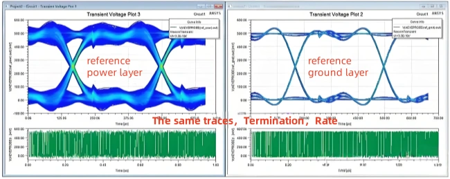
5. Choosing Between GND and Power as a Reference Plane
Both power and ground planes can be used as reference planes. They both give some shielding. But power planes have higher impedance and more voltage differences. This makes them less good for shielding. Ground planes have a constant voltage and are the better choice.
Still, sometimes real projects use power planes as reference planes. For example, in an ADAS project, PDN simulations kept failing. Then they changed part of the surface GND to a power plane. High-speed signals on layer 3 then used the power plane as a reference. The PDN simulation then passed. Even though this method did not follow standard rules, it worked in real life and led to debates among the engineers.
6. The Structure of PCB Layer Stacking
Each power, signal, and ground layer is covered by an FR4 dielectric layer. The thickness of the dielectric between layers is important. The PCB laminate has two materials: Core and PP.
Core: Also called the board core, it is the basic material for multilayer PCBs. It is a hard board with copper foil on both sides. It can be used as a signal layer, power layer, or ground layer. The core is solid and gives good strength and electrical properties.
PP (Prepreg): This is short for “Prepreg” and is also called a semi-cured sheet. It is a partly solid resin made mostly of fiberglass and epoxy. It fills gaps and acts as glue in PCB making. When the board is made, PP melts, flows, and hardens, bonding the layers and making an insulator. PP does not have copper foil on its surface and is softer. In multilayer PCBs, PP fills gaps between Core layers. Often, PP has a copper foil on one side, so it is called a “semi-cured sheet.”
Basically, PP is like FR4 with one copper layer, and Core is FR4 with copper on both sides. This is why PCBs usually have an even number of layers. The Core is usually thicker than PP. For example, in a 4-layer, 1-step HDI board, the Core is much thicker than PP. This makes the ground plane close to the signal layer, which improves EMC by giving better signal shielding.
7. EMC Considerations in PCB Design
In Electronic Design Automation (EDA), to get better EMC, follow two rules for dielectric thickness:
The thinner the space between the signal layer and the ground layer, the better.
The thicker the space between two signal layers, the less they interfere with each other.

8. Physical Symmetry vs. Signal Layer Symmetry
PCB making uses lamination technology. This means the dielectric and copper layers must be the same on both sides. For example, in an 8-layer, 2-step board, the copper thickness is the same on opposite sides:
Layer 1 and Layer 8: 30μm
Layer 2 and Layer 7: 20μm
Layer 4 and Layer 5: the same thickness
The same goes for PP thickness. If PP1067 is used between Layers 1-2 and 7-8, use it between Layers 2-3 and 6-7 too.
In through-hole PCBs, the layers are usually symmetric. For example, in a 6-layer through-hole PCB:
Layer 1 and Layer 6 are signal layers.
Layer 2 and Layer 5 are ground layers.
Layer 3 and Layer 4 are power layers.
But in HDI boards, keeping signal layer symmetry is harder. For example, in a 6-layer, 1-step HDI board, routing from Layer 1 to Layer 4 needs vias through Layers 2 and 5. This makes it hard to make Layer 2 a ground layer. So, Layer 3 is used as GND. Symmetry would need Layer 4 to be GND too, which wastes space. So, signal symmetry in HDI boards is hard to achieve.
Note for Interviews:
If someone asks for a 6-layer PCB stack-up, saying “S1-S2-G-S3-S4-S5” is wrong because it does not follow the symmetry rule.
9. 4-Layer PCB Stack-Up
2-layer PCBs do not have separate power and ground planes. So, we use 4-layer PCBs. There are three common stack-up types.
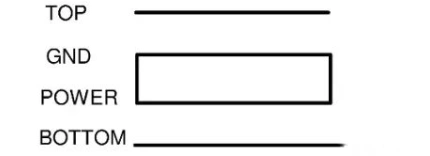
Option 1 (Preferred)
Layer 1 (Top): Signal
Layer 2: Ground (GND)
Layer 3: Power
Layer 4 (Bottom): Signal
Suggestions:
Route impedance-controlled traces on the outer layers, using Layer 2 (GND) as a reference.
Make the space between Power and GND as thin as possible to lower impedance and improve decoupling.
Option 2 (For Shielding)

Layer 1: Ground
Layer 2: Signal
Layer 3: Power
Layer 4: Ground
Problems:
Big gap between power and ground raises impedance.
Component pads can break ground/power planes.
Impedance gaps can cause signal reflections.
This option is only for boards with few components where shielding is most important.
Option 3 (Alternative)
This is like Option 1 but is changed for placing components on the bottom side.

10. 6-Layer PCB Stack-Up
A 6-layer PCB should have two ground planes. There are four common types. Option 3 is best:
| Option | Power | Ground | Signal | Layer 1 | Layer 2 | Layer 3 | Layer 4 | Layer 5 | Layer 6 |
|---|---|---|---|---|---|---|---|---|---|
| 1 | 1 | 1 | 4 | S1 | G | S2 | S3 | P | S4 |
| 2 | 1 | 1 | 4 | S1 | S2 | G | P | S3 | S4 |
| 3 | 1 | 2 | 3 | S1 | G1 | S2 | G2 | P | S3 |
| 4 | 1 | 2 | 3 | S1 | S1 | P | G2 | P | S3 |
Layer 1: Signal
Layer 2: Ground (GND)
Layer 3: Signal
Layer 4: Power
Layer 5: Ground (GND)
Layer 6: Signal
Why Option 3?
It keeps power and ground close to lower impedance.
It gives good EMC performance.
For designs that need to save money, Option 1 can be used.
11. 8-Layer PCB Stack-Up
For 8-layer PCBs, try to use three ground planes. There are five options. For a single power plane, Option 2 is better than Option 1. It reduces nearby signal layers and improves power-ground connection. For two power planes, Option 3 is recommended. It gives:
| Option | Power | Ground | Signal | Layer 1 | Layer 2 | Layer 3 | Layer 4 | Layer 5 | Layer 6 | Layer 7 | Layer 8 |
|---|---|---|---|---|---|---|---|---|---|---|---|
| 1 | 1 | 2 | 5 | S1 | G1 | S2 | S3 | P | S4 | G2 | S5 |
| 2 | 1 | 3 | 4 | S1 | G1 | S2 | G2 | P | S3 | G3 | S4 |
| 3 | 2 | 2 | 4 | S1 | G1 | S2 | P1 | G2 | S3 | P2 | S4 |
| 4 | 2 | 2 | 4 | S1 | G1 | S2 | P1 | P2 | S3 | G2 | S4 |
| 5 | 2 | 2 | 4 | S1 | G1 | P1 | S2 | S3 | G2 | P2 | S4 |
No signal layers next to each other,
Symmetry in layers,
Close power and ground.
Other options (4 and 5) can be used if design needs are different.
12. 10-Layer PCB Stack-Up
For 10-layer PCBs, use four ground planes. Common setups are:
| Option | Power | Ground | Signal | Layer 1 | Layer 2 | Layer 3 | Layer 4 | Layer 5 | Layer 6 | Layer 7 | Layer 8 | Layer 9 | Layer 10 |
|---|---|---|---|---|---|---|---|---|---|---|---|---|---|
| 1 | 1 | 3 | 6 | S1 | G1 | S2 | S3 | G2 | P | S4 | S5 | G3 | S6 |
| 2 | 1 | 4 | 5 | S1 | G1 | S2 | G2 | S3 | G3 | P | S4 | G4 | S5 |
| 3 | 2 | 3 | 5 | S1 | G1 | S2 | P1 | S3 | G2 | P2 | G3 | S4 | G4 |
| 4 | 2 | 4 | 4 | S1 | G1 | S2 | G3 | P1 | G2 | P2 | G3 | S3 | S4 |
Option 3 (Best Choice):
It makes Layers 3-4 and 7-8 farther apart and Layers 5-6 closer. This setup is good for performance and cost.
Option 4:
Gives the best EMC performance but loses one routing layer.
For a single power plane, Option 2 is preferred. Option 1 is cheapest but has more signal layers next to each other.
Related Posts
PCBA Prototype
December 8, 2025
PCBA Prototype
November 9, 2025


