Silkscreen Design and Adjustment for PCB Assembly

For later component assembly and manual assembly, a PCB assembly drawing is made for component placement. Then the silkscreen reference designators are needed.
Many new PCB designers adjust the silkscreen reference designators by hand one by one. This work is boring and slow.
Is there a better way?
In production, you can show or hide the silkscreen layer without changing the assembly drawing. Press the shortcut key “L” and click the button to turn off all layers. Then turn on only the silkscreen and matching solder mask layers. This lets you adjust the silkscreen.
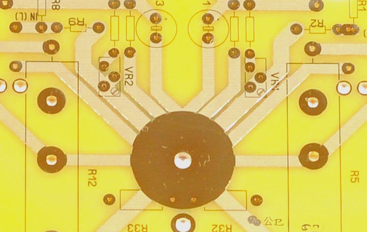
Here are the rules and suggested sizes for silkscreen reference designators:
Do not let the silkscreen overlap the solder mask. Overlap may make the silkscreen disappear in production.
The silkscreen must be clear. Use text sizes of 4/25mil, 5/30mil, or 6/45mil for width and height.
Keep the orientation the same. Do not use more than two directions on one board. Place letters on the left or bottom of components.

For designators placed awkwardly because of layout limits, use 2D lines or boxes to mark them so they are easier to read (see Figure 11-22).

Methods to Adjust Silkscreen Reference Designators
Altium Designer gives a fast way to change the silkscreen. Use the “Component Text Placement” feature. It lets you put designators around or inside components quickly.
Step 1: Select the components you want to change.
Step 2: Press the shortcut key “AP” to open the “Component Text Placement” dialog box. The box gives options for “Designator” and “Comment”. Use “Designator” as an example.

Step 3: You can place the designator in these directions: Up, Down, Left, Right, Top-Left, Bottom-Left, Top-Right, or Bottom-Right. They match the keys on the number pad. For example, to put a designator above a component, press “5” then “2” . To put it on the right, press “5” and “6”. To put it below, press “5” and “8”.

PCB Design Tips
How to Choose PCB Substrate Materials?
You must balance design needs, production, and cost. The design needs have electrical and mechanical parts. For high-speed PCBs (over GHz), material choice is very important. FR-4 may show high dielectric loss at GHz frequencies and hurt signal quality. Check the dielectric constant and loss at your working frequency.How to Avoid High-Frequency Interference?
Keep high-frequency interference low by reducing crosstalk. Increase the distance between high-speed and analog signals. Use ground guards or shunt traces near analog signals. Watch digital ground noise on analog ground.How to Ensure Signal Integrity in High-Speed PCB Design?
Signal integrity problems come from impedance mismatch. Main factors are the source’s impedance, trace impedance, load, and layout. Fix these with correct termination and routing.Can a Ground Line Be Added Between Differential Pairs?
No. A ground line between differential pairs breaks their coupling and cancels benefits like noise immunity.Should Shield Ground Lines Be Added to Both Sides of Clock Traces?
This depends on EMI and crosstalk. Bad shield ground lines can make things worse.In Allegro, What Causes Short Wire Segments with Small Boxes During Routing?
These come from automatic groups when reusing modules. To fix, break the group in “Placement Edit” mode and then move each small box.How to Meet EMC Requirements Without High Costs?
Extra ground layers, ferrite beads, and chokes raise costs. To lower EMI, you can:Use components with slower edge rates to lower high-frequency noise.
Keep high-speed parts away from external connectors.
Make sure impedance matches and return paths are good to reduce reflection and radiation.
Use proper decoupling capacitors at power pins to lower noise in power and ground.
Connect the ground near connectors to the chassis ground.
Use guard traces if needed, but note that they affect trace impedance.
Make the power plane 20H smaller than the ground plane, where H is the gap between them.
What Are the Rules for Microstrip Design in RF PCBs (Above 2GHz)?
Use 3D field analysis tools to get parameters. Follow the rules from the field solver.Should AC Coupling Capacitors Be Closer to the Transmitter or Receiver?
It depends on the case:Follow design guidelines if given.
For IC-to-IC, put it near the receiver.
For IC-to-connector, put it near the connector.
AC coupling capacitors do these things: they block DC differences, remove DC bias to improve signals, and protect from DC bias and overcurrent. They make the signal even around 0V and help with noise. They can also cause impedance changes and slow signal edges.
How to Check if a PCB Meets Manufacturing Requirements Before Delivery?
Most PCB makers do electrical tests before shipping to check that all nets are correct. Many use X-ray to find etching or lamination errors. For assembled boards, they use ICT, which needs test points in the design. If problems occur, advanced X-ray tools can show if they are due to production errors.
Table of Contents

Related Posts
PCBA Prototype
April 27, 2026
PCBA Prototype
April 14, 2026