PCB Basics 2 Vias – GREATPCB PCB and PCBA Manufacturer

—Common Classifications of Vias—
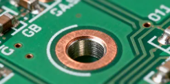
Through-holes are connection holes between the top and bottom layers of a PCB , and these holes also provide interconnection between internal PCB layers.
Blind vias are vias that connect the surface layer and the inner layer without penetrating through it. They are used for interconnection between the top or bottom layer of a PCB and the inner PCB layers.
Buried vias are vias that connect inner layers and are not visible on the surface, used for interconnection between internal PCB layers.

PCB
—Location of via—
Vias should not be designed on pads; they should be connected by a short section of printed trace. Otherwise, defects such as ” stacks ” and ” insufficient solder ” may occur . If solder resist is applied to the via pads, the distance can be as small as 0.1mm ( 4mil ).
Vias cannot be designed at the center of the pads of surface mount components on the soldering surface.
—Through-hole treatment method—
Green oil cover ( Tented Via )
The via surface is completely covered by solder mask, with only the pad exposed.
Prevent dust and moisture from entering the hole;
Reduce the risk of via oxidation;
Improve electrical insulation;
To prevent solder balls from entering the hole during soldering.
Open the window ( via in Pad / Exposed Pad )
The via surface is not covered with solder mask, and the copper layer is directly exposed.
It can be used as a test point;
Increase the heat dissipation area;
This facilitates later maintenance and measurement.
—Parasitic parameters of vias—
parasitic capacitance
Each via has a parasitic capacitance to ground relative to the ground plane. An electric field exists between the via and the surrounding ground plane or other conductive layers, thus creating parasitic capacitance. Capacitive effects exist between the via pads and the gaps on the ground plane, as well as between the via and adjacent conductive layers.
The basic formula for via parasitic capacitance:
Where C is the parasitic capacitance of the via ( pF ); D2 is the diameter of the via on the ground plane ( in inches); D1 is the diameter of the pad surrounding the via ( in inches); T is the thickness of the printed circuit board ( in inches); and εr is the relative permittivity of the circuit board.
Generally speaking, the thicker the circuit board, the larger the pad diameter, and the smaller the difference between the aperture diameter and the pad diameter, the larger the parasitic capacitance.
At low frequencies, parasitic capacitance is very small and can be completely ignored. In high-speed digital circuits, the main effect of via parasitic capacitance is to slow down or degrade the rise time of digital signals. Therefore, the parasitic capacitance of vias needs to be strictly controlled in the PCB design of high-speed digital and radio frequency circuits.
Optimization measures
- By properly controlling the size of pads and vias, parasitic capacitance can be reduced.
- Adding grounding vias around high-speed signals helps improve signal shielding and reduce crosstalk caused by parasitic capacitance.
- By making reasonable use of the interlayer structure of multilayer boards, optimizing the layout of power and ground layers, and reducing the electric field between vias and surrounding conductive layers, parasitic capacitance can be reduced.
Parasitic inductance
Each via has a parasitic series inductance. When current flows through a via, a magnetic field is generated around it, thus creating an inductive effect. A via can be viewed as a tiny wire, and the magnetic field around the wire stores energy, which is equivalent to the existence of an inductance.
The basic formula for via parasitic inductance:

Where L is the via inductance (in nH ); h is the via length ( in inches); and d is the via diameter ( in inches).
For high-speed digital circuits and radio frequency circuit PCB design, the parasitic inductance of vias cannot be ignored.
For example, in a power bypass circuit of an integrated circuit, a bypass capacitor is connected between the power plane and the ground plane, with the expectation that the high-frequency impedance between the power plane and the ground plane will be zero. However, this is not the case in reality. Each via inductance connecting the capacitor to the power plane and the ground plane introduces a small but measurable inductance ( in the nH range). The via series inductance reduces the effectiveness of the power bypass capacitor, degrading the overall power supply filtering performance.
Reference book: Printed Circuit Board (PCB) Design Technology and Practice
Optimization measures
- Minimize the length of vias and increase their diameter to reduce parasitic inductance.
- Adding grounding vias around high-speed signals can reduce the inductance of the signal loop and mitigate the effects of parasitic inductance.
—Supplement to proper nouns—
Gold fingers are conductive contacts on the edge of a PCB , used for the physical and electrical connection between the board and its slot. They are commonly found in devices such as graphics cards, memory, and expansion cards.
- Location: PCB edge, usually arranged on one or both sides.
- Shape: Rectangular conductive area, often with beveled edges.
Coating type
- Hard gold ( electrolytic nickel gold )
- Soft gold ( immersion gold )
Read More: Why Choose Quick Turn PCB Boards for High-Precision LED Applications?
Related Posts
PCBA Prototype
December 30, 2025
PCBA Prototype
December 20, 2025


