SMD and NSMD

- Definition
(1)SMD Pad
SMD pad(pressure pad design)
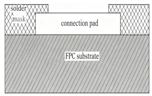
Explanation: The solder mask defines the pad size(Solder Mask Defined Land Pattern).The opening in the solder mask is smaller than the pad, commonly referred to as a pressure pad design in FPC.
Pressure Pad Design
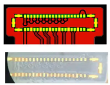
(Final product effect diagram, pad length are the same, less likely to break)
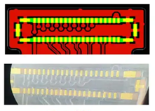
Pressure Pad Design
(Final product effect diagram, pad length are the same, avoids SMT staking issues)
(2)NSMD Pad

#NSMD pad(non-pressure pad design)
Copper defines pad size(Non Solder Mask Defined Land Pattern or Copper Defined Land Pattern).Also called non-mask defined pad. The solder mask opening is larger than the pad. In FPC, this is known as a non-pressure pad design.

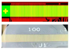
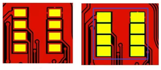
Non-pressure pad design
(final product effect diagram, pad lengths are not the same, easy to break)
Non-pressure pad design
(final product effect diagram, pad lengths are not the same, easily causes SMT standing issues.
- Solder Joint Pull Force
The solder joint pull force is the combination of the solder paste and the solder pad.

In the SMD(Surface Mount Device)diagram, the copper pad area is large, but it is covered by a solder mask on the sides, so only one side joins in the soldering. In the NSMD(Non-Solder Mask Defined)diagram, the copper pad is all around, so it joins on three sides, which is more than SMD. So, the solder joint is greater.
But in PCB(Printed Circuit Board) or FPC(Flexible Printed Circuit)production, NSMD pads are relatively independent and can be over-etched or side-etched. It’s important to compensate the pads properly, or the pads will be too small, which will affect the solder joint strength and pull force.
- Solder Joint Pull Force
The solder joint pull force is the combined strength of the component after soldering with the PCB or FPC base material.
#SMD Pad Design| NSMD Pad Design
The SMD pad has a large copper area. Although the exposed area is the same as the NSMD pad, the actual contact area with the base material is much larger. So, the SMD pad has a much better combination with the base material. The pad is more secure and less likely to fall off.
FPC uses a covering layer as a solder mask. If using SMD pad design, the covering layer can press down on the pad area, which is called a “pressed pad design.”This makes the pad and base material more secure.
- Pros and Cons Comparison
(1)SMD
1) Advantages
- The pad shape is neat and not affected by wiring, suitable for small parts like 0402,0201,etc.
- Less likely to crack or fall off during repair because the actual copper size of SMD pads is larger compared to NSMD, and the green solder mask covers part of the pads.
2) Disadvantages
- The green solder mask covers the pads, making the steel mesh higher than NSMD by the thickness of the green solder mask, increasing the amount of solder, which can cause shorts during production.
- Reduces the copper surface area for pad connections and decreases the space between pads.
- The solder strength of SMD pads is relatively weaker.
(2)NSMD
1) Advantages
- Larger solder area, relatively stronger solder strength.
- More space between pads, allowing for wider traces and more vias.
2) Disadvantages
- The shape of the pad is affected by the wiring.
- NSMD pads are standalone and can easily fall off during repair.
- Choose the Right Pad
- For PCB, it’s better to use NSMD pads, but for BGA and small pads, like those smaller than 0201 packages, it’s recommended to use SMD pads to prevent pads from falling off during repair.
- For FPC, it’s better to use SMD pads. The solder mask can press around the pad, supporting the pad strength and preventing it from falling off.
Table of Contents

Tags
Related Posts
PCBA Prototype
July 17, 2026