Experience Formulas in PCB Design

In PCB design rules, there are numerous empirical formulas for designers to reference. However, is there a simpler method to address practical issues?

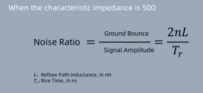
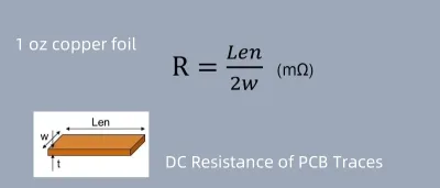
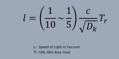


Even if a ground copper plane has no DC resistance, it still exhibits impedance under AC signals. The desired signal is what it is; the unwanted signal is noise. Noise only differs in magnitude and cannot be completely eliminated. To completely eliminate noise, you must also eliminate the signal.
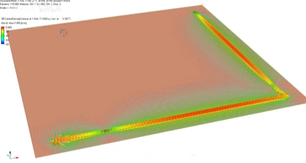
Example Analysis
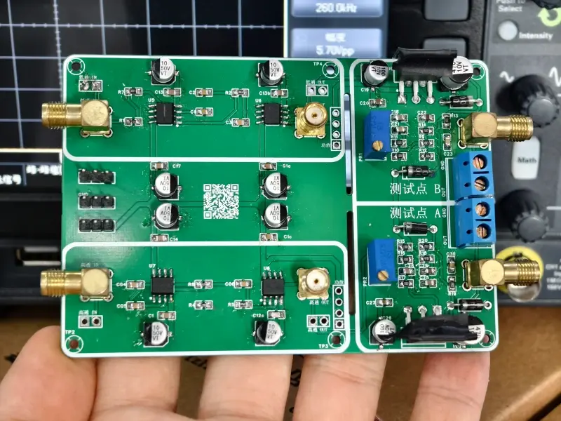
As shown in the diagram, the power supply is at the top of the PCB, and the high-frequency power amplifier is at the bottom. Due to the power connector and amplifier heatsink, this layout is common. Assuming a complete ground plane, it is anticipated that high-frequency currents will flow back to the power ground through this plane.

If there are sensitive circuits in the upper right corner of the PCB, they will inevitably be affected by this high-frequency return current. A common solution is to isolate the ground of the sensitive circuit area and use a single-point ground. This way, high-frequency interference currents from the ground plane will not flow into the sensitive circuit area, or only minimally.

Cost and Trade-offs
This method is not without cost. After isolating the ground plane, the original high-frequency current path becomes smaller, and impedance increases, leading to higher interference voltage in that area. Moreover, the isolated area on the ground plane effectively forms a slot antenna, increasing EMI radiation from the PCB. Therefore, in some cases, this method of ground plane isolation may be inappropriate and needs to be analyzed based on the specific situation; there is no one-size-fits-all solution.

Application of Empirical Formulas
When applying various empirical formulas, we find that qualitative analysis alone is insufficient for decision-making. Noise cannot be eliminated, but it can be minimized. How low should the noise level be to be acceptable? PCB traces can be made as short as possible but cannot be zero; how short is “short enough”? These questions require numerical judgment. This is why we still need formulas in empirical rules. Empirical formulas simplify the complex details of theoretical formulas, highlight the main issues, and incorporate application scenario parameters, often providing rough estimates without needing calculation software or calculators. In this context, precision is less critical than speed and simplicity.
Ground Bounce Issue Analysis
What is Ground Bounce?
Ground bounce refers to interference that occurs on the ground line when high-frequency currents flow through a return path with high parasitic inductance. This interference voltage is commonly referred to as ground bounce.
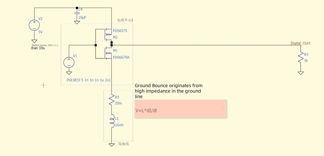
Problems with Multiple Signals Sharing a Return Path
If multiple signals share a return path in a circuit, ground bounce noise from one signal can interfere with other signals. The more digital signals output simultaneously, the greater the variation in current within the shared return path, leading to increased ground bounce noise. The ground bounce voltage of the signal return path can be calculated using the formula:
Vnoise=L⋅dIdtV_{noise} = L \cdot \frac{dI}{dt}Vnoise=L⋅dtdI
Next, determine the inductance of the return path:

For a 50Ω transmission line loop inductance, the empirical formula is:

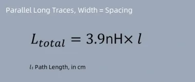
For parallel signal lines and return paths, if the trace width equals the trace spacing, the total inductance is:
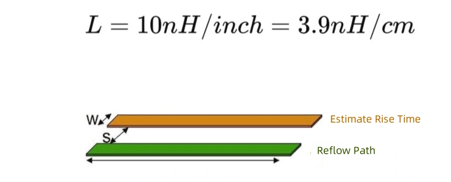
This empirical rule can be used to estimate the inductance of socket or IC pin traces. If there is a large area of copper around the traces or the spacing does not match the trace width, a 2D electromagnetic field solver is needed.

Considering Signal Frequency and Bandwidth
Frequency and bandwidth are key factors in applying PCB design rules. Higher signal frequencies make the effects of skin effect, trace parasitic inductance, capacitance, and dielectric parameters more pronounced. When calculating or estimating signal bandwidth, note that digital signal data rate and analog signal bandwidth are different concepts and not equal in value.
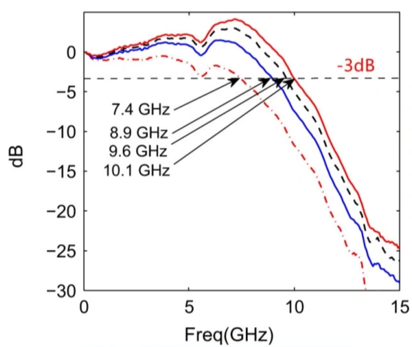
Definition of Signal Bandwidth
Signal bandwidth refers to the width of the frequency range occupied by the signal. If the transmission line bandwidth is less than the signal bandwidth, signal distortion will occur. Digital signal bandwidth is related not only to data transmission rate but also to rise and fall times.
Formula
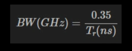
where:
- TrT_rTr is the rise time from 10% to 90% (in ns)
- BWBWBW is the signal bandwidth (in GHz)
Signal bandwidth can be roughly considered as the highest frequency component of the signal or the highest frequency needed to reconstruct a waveform with rise time TrT_rTr. This helps us consider signal characteristics in the circuit.
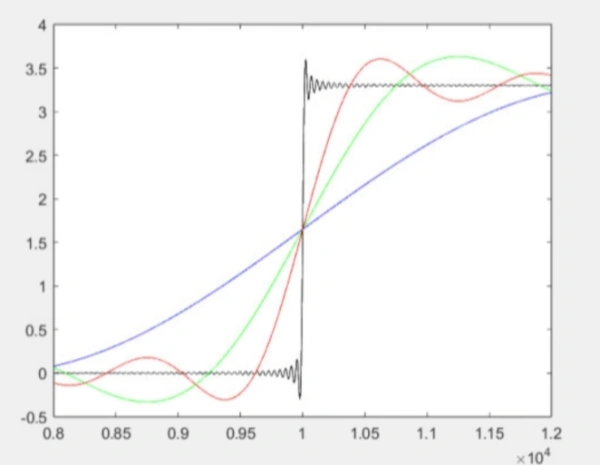
Frequency and Bandwidth Relationship
For example, with a rise time of 1 nanosecond, the highest sinusoidal frequency component of the signal is 350 MHz; with a rise time of 350 ps, the signal transmission line bandwidth must exceed 1 GHz to ensure the rise time is not damaged.
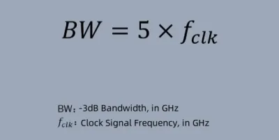
For clock signals with a constant frequency, the bandwidth can be estimated using the empirical formula:

Similarly, clock signal bandwidth is determined by rise time, not clock frequency. Clock signals with the same frequency but different rise times have significantly different bandwidths.
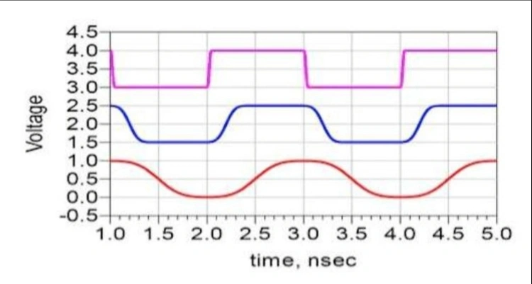
If the rise time parameter of the clock signal is not available, use the empirical rule:
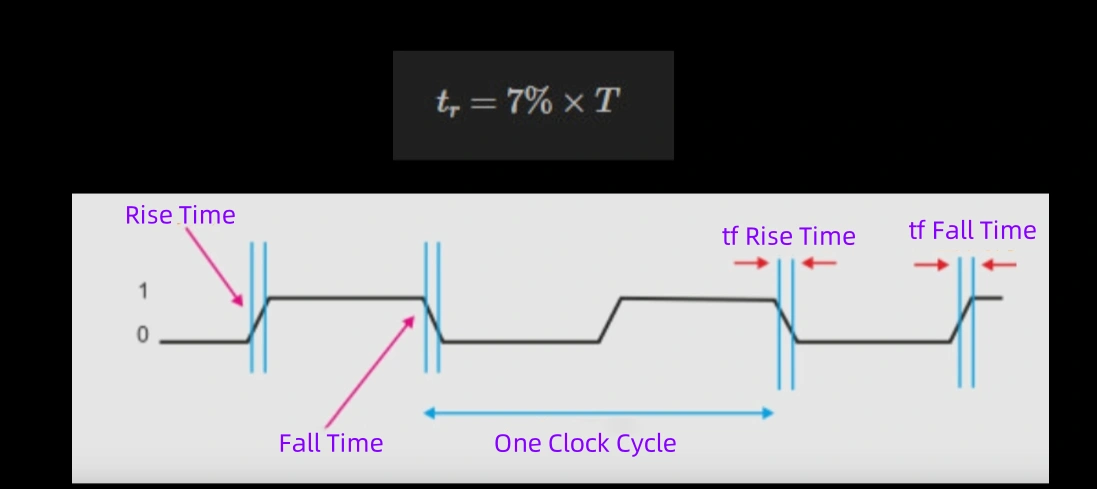
T represents the time period. This is a relatively conservative estimate, and the estimated rise time might be slightly smaller than the actual. Once the rise time is known, the bandwidth of the clock signal can also be estimated using the following formula: the bandwidth of the clock signal is five times its frequency.

Example Calculation
Common question: What is the bandwidth for a USB 2.0 data transfer rate of 480 Mbps?
Most serial signals use NRZI encoding with two bits per cycle, resulting in a potential clock frequency of half the bit rate. Therefore, for a 480 Mbps signal, the clock frequency is 240 MHz, and the signal bandwidth is 1.0 GHz.

Summary
In PCB design, empirical formulas provide practical references for addressing real-world issues. While it’s not possible to completely eliminate noise, it can be minimized through proper design and isolation. Key factors include ground bounce issues and signal bandwidth calculations. Empirical formulas simplify complex computations, aiding designers in quick estimations and optimizations.


