PCB Surface Treatment Plating Process
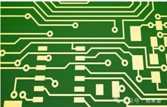
Introduction: PCB plating processes require careful attention . It ‘s more than just applying a random layer of coating . First, it protects copper wires from oxidation . Copper easily oxidizes in air, which can easily lead to problems like cold joints and false solder joints. Second, it provides a good soldering surface. The plating process provides a good soldering surface and a wear-resistant, low-resistance connection surface for the contact points. Different plating processes have their own advantages and disadvantages regarding price, surface flatness, and solderability, and the choice should be tailored to the application scenario.

#pcb-design
Technical Comparison
HASL :
Process: Immerse the PCB in molten lead-tin solder, then use a high-temperature hot air knife to blow away excess solder to obtain a flat, uniform solder coating.
Advantages: Lowest cost , excellent welding performance, strong solder joints , and mature technology.
Disadvantages: Not suitable for high-density, fine-pitch components (such as BGA) ; high-temperature processes may cause stress on the board, leading to deformation or potential defects ; traditional lead-containing HASL cannot be used due to environmental protection ( RoHS) requirements , and lead- free HASL can be used .
Applications: low-cost consumer electronics and printed circuit boards with low requirements for surface flatness
Immersion Gold ( ENIG ) – Immersion Nickel Gold:
Process: First, a layer of nickel-phosphorus alloy is chemically deposited on the copper surface (as a barrier layer and solderable layer), and then a thin layer of gold is deposited on the nickel layer through a chemical replacement reaction.
Nickel layer: It is the main body, provides solderability and forms a diffusion barrier with copper.
Gold layer: extremely thin (usually 0.05-0.1μm), only used to protect the nickel layer from oxidation during storage. During welding, the gold will quickly dissolve into the solder, exposing fresh nickel for welding.
Advantages: Smooth surface suitable for fine-pitch BGA, QFN, QFP and other components ; good oxidation resistance and long shelf life ; suitable for wire bonding .
Disadvantages : High cost ; risk of “black pad” (black pad). Due to improper process control, the nickel layer can be excessively corroded, forming a fragile phosphorus-rich layer, causing brittle fracture of the solder joint and reduced reliability. This is the biggest risk of ENIG .
Applications: mid-to-high-end products such as smartphones , communication equipment , and medical electronics.
Immersion Silver :
Process: A layer of silver is deposited on the copper surface by chemical replacement ; copper atoms displace silver ions from the solution, forming a layer of silver on the surface.
Advantages: Smooth surface ; very good solderability; cost between OSP-organic solderability preservative and ENIG-immersion gold process.
Disadvantages: It is easily oxidized and sulfurized , and will turn yellow (oxidation) or black (sulfurization) when exposed to air, and has high requirements for packaging and storage ; there is a risk of silver migration. In high temperature and high humidity environments, ion migration may occur under the action of the electric field, leading to insulation failure (modern formulas have greatly improved this problem).
Applications: communication products, automotive electronics, etc
Immersion Tin :
Process: A layer of tin is deposited on the copper surface through chemical replacement , similar to immersion silver, and the copper replaces the tin ions .
Advantages: Very smooth surface; excellent compatibility with tin solder.
Disadvantages: Tin whisker risk: Tin layers can spontaneously grow tiny whiskers under internal stress, causing short circuits. This needs to be suppressed through additives and process control. Scratch resistance and low hardness. Short shelf life.
Application: Mainly used in certain specific fields such as automotive electronics.
Hard Gold / Electrolytic Hard Gold :
Process: It is not used for welding, but for electrical connection . A thicker (usually >0.5μm), harder, and wear-resistant cobalt-gold or nickel-gold alloy is electroplated on the nickel barrier layer .
Advantages: extremely wear-resistant, low and stable contact resistance.
Disadvantages: Very high cost (thick gold layer); need to design electroplated leads, which makes the design more complicated; poor solderability because too thick a gold layer can cause gold brittleness.
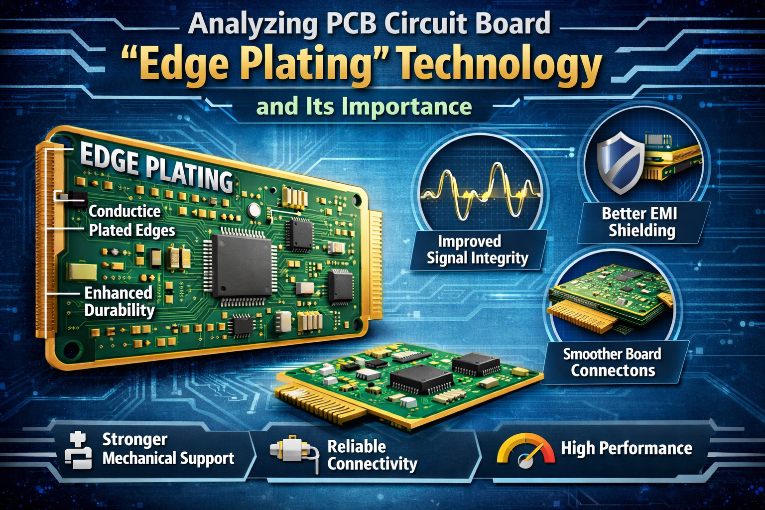
Application: Gold fingers (such as memory sticks, graphics card sockets), switch contacts, test points and other parts that require frequent plugging and unplugging or friction.
Chemical Nickel Palladium Gold ( ENEPIG ):
Process: An upgraded version of ENIG, known as the “universal” surface treatment ; an extremely thin palladium layer (Pd) is added between the chemical nickel layer and the immersion gold layer .
Palladium layer: It can perfectly prevent nickel corrosion and completely eliminate the ” black disk ” phenomenon; at the same time, palladium itself can be welded and can undergo a eutectic reaction with gold to form a stronger interface.
Advantages: Completely solves the black disk problem and is extremely reliable; also suitable for welding and punching gold and aluminum wires, with the widest range of applications.
Disadvantages: Highest cost (due to the use of precious metal palladium).
Applications: Fields with extremely high reliability requirements, such as aerospace and military electronics; and packaging that requires simultaneous welding and chip bonding (such as COB) .
Organic Solderability Preservative ( OSP – Organic Solderability Preservative ):
Process: An organic film grows on the surface of water copper , and a thin and uniform organic protective film is formed on the clean copper surface by chemical methods.
Advantages: The surface is very flat, perfect for fine-pitch components; low cost, cheaper than ENIG and other processes; the process is simple and environmentally friendly, involving only water washing and drying, and no heavy metals.
Disadvantages: The protective layer is thin and easily scratched, requiring careful handling; it cannot withstand multiple reflow soldering; the shelf life is short, usually 6 months; it is transparent and difficult to detect: it is difficult to inspect and needs to be removed before rework.
Application: For mass-produced consumer electronic products (such as computer motherboards and mobile phones), this is a cost-effective lead-free process.
Summary
For example: the price of tin spraying is three times that of immersion gold process. The thicker the immersion gold is, the more expensive it is. After all, the price of gold is there.
For conventional RF boards, immersion nickel gold (IGN) is sufficient. Low-frequency control boards with BGA packaged components also require immersion nickel gold. For very conventional low-frequency printed boards, tin spraying can be used.
Gold plating is typically used for RF boards involved in microassembly. This thickness is determined by the project’s requirements and the environment in which it will be used. Consult with the process designer to confirm the thickness. Localized thick gold treatment is also possible. For example, on 4350B PCBs , pads requiring gold wire bonding can be treated with this treatment.
PCB plating is a key process that gives PCBs vitality and reliability. Selecting the appropriate plating process based on the product’s application scenario (cost, performance, and environmental requirements) is a very important decision in PCB design and manufacturing.
For some mass production projects, choosing the right surface treatment process can save tens or even millions while ensuring product reliability.
Tags
Related Posts
PCBA Prototype
February 8, 2026
PCBA Prototype
February 1, 2026


