What is a High Frequency PCB?

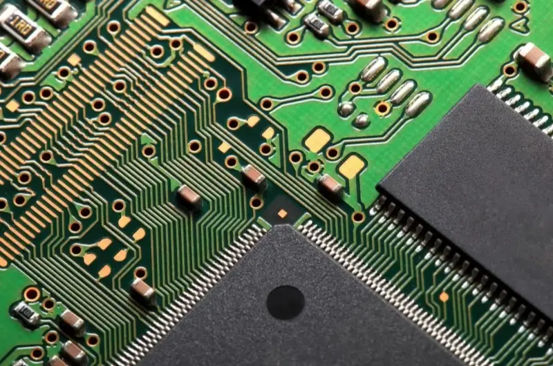
High-frequency PCB is a special circuit board that processes signals with higher electromagnetic frequency. Its manufacturing may be made by the ordinary rigid circuit board manufacturing method or after special treatment. In general, we can define high-frequency boards as PCB boards above 1GHz. PTFE materials are widely used in high-frequency PCB manufacturing, or Teflon, with frequencies above 5GHz.
Characteristics of High-Frequency PCB
- High-frequency characteristics: the signal delay and phase offset are small, suitable for the transmission of high-frequency signals, and can ensure signal integrity.
- High-speed transmission: strong performance, to meet the needs of high-speed data transmission.
- Manufacturing precision: the manufacturing process requirements are high, and the a need to ensure the accuracy and stability of the circuit board.
- Low noise: less noise interference, to ensure the stability of the signal.
- Good thermal stability: maintain stable performance in high-temperature environments, with good thermal stability.
The materials of PCB high-frequency PCB printing are mainly as follows:
- Substrate material: The substrate materials of high-frequency boards mainly include FR 4, CEM-1, aluminum substrate, etc. FR 4 is a common substrate material, with good electrical and mechanical properties, and the price is relatively cheap.
- Prepreg: prepreg is an intermediate material used for the manufacture of laminate. Its materials mainly include (PI), polyester (PET), and so on.
- Copper foil material: Copper foil is the basic material of the electronic circuit board. Its main materials are electrolytic copper foil and calendering copper foil. Electrolytic copper foil has good electrical conductivity and ductility but has poor thermal resistance and mechanical strength.
- Cover film material: The cover film is used to protect the circuit from the external environment. Its materials mainly include (PI), polyester (PET), and so on.
High-frequency PCB layout:
The high-frequency PCB manufacturing process is complex, and the unit cost is higher, which requires the PCB layout, in addition to choosing the appropriate number of PCB layers, but also a reasonable circuit board components layout planning, and using the appropriate wiring rules to complete the PCB design.
- The less the alternate lead between the layers of the high-frequency circuit, the better.
The less Via used when connecting, the better. A Via will bring a distributed capacitance of about 0.5 pF, reducing the number of Via can significantly improve the speed and reduce the likelihood of data errors.
- Lead lines between pins of high-frequency circuits.
The radiation intensity of the signal is proportional to the leading length of the signal line. The longer the high-frequency signal leads, the easier it is to couple to its components. Therefore, for the signal clock, crystal vibration, DDR data, LVDS, USB, HDMI, and other high-frequency signal lines, the leading length is the shorter, the better.
- Bending between the pins of high-frequency electronic devices.
High-frequency electrical wiring lead preferably adopts a full straight line, which is only to improve the binding strength of copper foil in low-frequency circuits, and in high-frequency circuits, meeting this requirement can reduce the external emission and coupling of the high-frequency signal.
Application:
High-frequency boards are widely used in wireless communication, network equipment, aerospace, military and medical equipment, and other fields. For example, in satellite communications, the high-frequency board is used to process signal transmission from ground to orbital satellite; in medical devices, especially imaging devices such as MRI, the high-frequency plate is used to process complex signal information.
Table of Contents
Related Posts
PCBA Prototype
September 24, 2024
PCBA Prototype
September 10, 2024


