Achieving Zero Defects: Quality Control in PCB Manufacturing
By PCBA PrototypePublished On: 2025-01-23Categories: PCB Design, PCB layout, PCBA, Services0 Comments on Achieving Zero Defects: Quality Control in PCB Manufacturing
By PCBA PrototypePublished On: 2025-01-23Categories: PCB Design, PCB layout, PCBA, Services0 Comments on Achieving Zero Defects: Quality Control in PCB Manufacturing

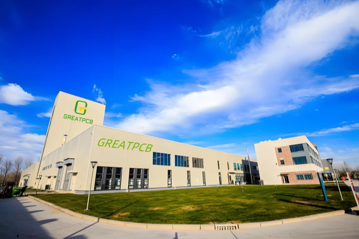
In the highly competitive world of Printed Circuit Board (PCB) manufacturing, achieving zero defects is not just a lofty goal but a necessity for survival and success. At GreatPCB, we have made zero defect management the cornerstone of our operations, ensuring that every PCB leaving our factory meets the highest quality standards.
The Significance of Zero Defect Management in PCB Manufacturing
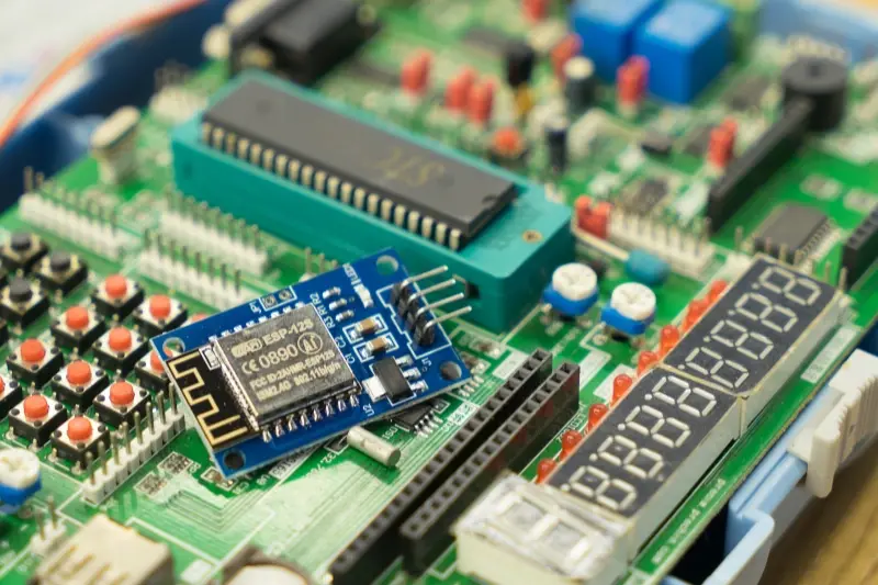
PCBs are the backbone of countless electronic devices, from smartphones and laptops to complex industrial machinery and aerospace equipment. A single defect in a PCB can lead to device malfunctions, reduced performance, and even safety hazards. Therefore, implementing zero defect management is crucial to enhance product reliability, reduce costly rework and recalls, and ultimately, boost customer satisfaction.
Quality Control in Design Phase
Design for Manufacturability (DFM)
Our design team at GreatPCB is well – versed in Design for Manufacturability principles. We work closely with customers from the initial design concept, providing early feedback on potential manufacturing issues. By optimizing the design layout, component placement, and trace routing, we ensure that the PCB design is not only functional but also easy to manufacture with minimal errors. For example, we use advanced design software to analyze thermal performance, signal integrity, and power distribution, making adjustments to prevent overheating and signal interference problems during production.

Design Reviews
Before the design is finalized, we conduct comprehensive design reviews. Multiple experts from different fields, including electrical engineering, mechanical engineering, and manufacturing, come together to scrutinize every aspect of the design. This multi – disciplinary approach helps to identify and rectify any design flaws that could potentially lead to manufacturing defects. We also encourage customers to participate in these reviews, fostering a collaborative environment that ensures the final design meets both the customer’s requirements and our high – quality manufacturing standards.
Quality Control in Production Phase
Advanced Manufacturing Equipment
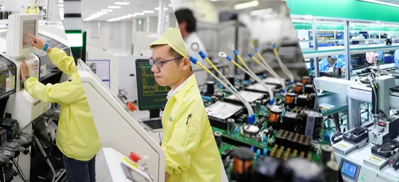
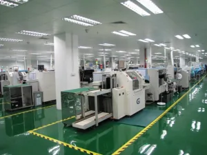
GreatPCB is equipped with state – of – the – art manufacturing equipment. Our automated surface – mount technology (SMT) lines are highly precise, capable of placing components with micron – level accuracy. This high – precision placement reduces the risk of component misalignment, soldering defects, and short circuits. In addition, our high – speed drilling machines can create holes with consistent quality, ensuring proper component insertion and electrical connection.
Stringent Process Control
We have established a series of strict process control measures in the production line. Each production process, from circuit board etching to soldering, is monitored in real – time. For example, we use automated optical inspection (AOI) systems to detect any defects in the solder joints, component placement, and circuit traces immediately after the SMT process. This allows us to identify and correct problems promptly, preventing defective products from proceeding further in the production line.
Employee Training and Quality Culture
Our employees are the key to our zero – defect success. We invest heavily in employee training, ensuring that every worker is well – trained in the latest manufacturing techniques and quality control procedures. We also foster a strong quality culture within the factory, where every employee is encouraged to take ownership of quality and report any potential issues immediately. This proactive approach to quality control has significantly reduced the defect rate in our production.
The GreatPCB Advantage
Comprehensive Service
At GreatPCB, we offer a one – stop solution for PCB manufacturing. From design assistance to prototyping, mass production, and final testing, we handle every aspect of the PCB manufacturing process. This integrated service not only streamlines the production process but also enables us to maintain strict quality control at every stage.
Customization
We understand that every customer has unique requirements. Whether it’s a high – density interconnect (HDI) PCB for a high – end smartphone or a rugged PCB for industrial applications, we have the expertise and flexibility to provide customized solutions. Our engineering team can work with customers to develop tailored PCB designs and manufacturing processes to meet specific performance, environmental, and cost – effectiveness requirements.
Competitive Pricing
Despite our commitment to zero defect management and high – quality manufacturing, we offer competitive pricing. By optimizing our production processes, leveraging our economies of scale, and continuously improving our efficiency, we are able to provide cost – effective solutions without compromising on quality.
Manufacturing Process Details
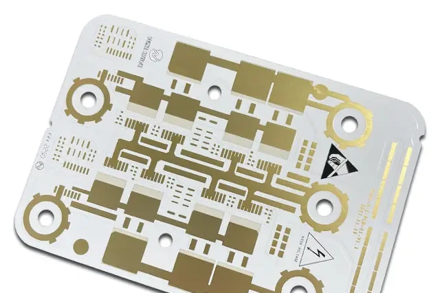
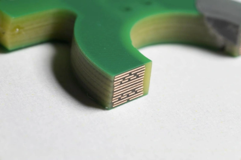
We take pride in our diverse manufacturing capabilities. Our double – sided and multi – layer PCB production can handle up to 20 layers, with a minimum line width/space of 3mil/3mil, ensuring high – density circuit designs. For rigid – flex PCBs, we use advanced lamination techniques to achieve seamless transitions between rigid and flexible areas, which is essential for applications in wearables and foldable devices. Additionally, we offer a wide range of surface finishes, including HASL (Hot – Air Solder Leveling), ENIG (Electroless Nickel Immersion Gold), and OSP (Organic Solderability Preservative), each with its unique advantages for different product requirements.
Customer Success Stories
To further illustrate our capabilities, we have numerous customer success stories. For instance, a leading automotive electronics company approached us with a complex PCB design for their new in – car infotainment system. The project required high – speed signal transmission, strict thermal management, and automotive – grade reliability. Our team worked closely with them from the design stage, optimizing the layout to meet their performance requirements. Through rigorous quality control during production, we were able to deliver the PCBs with zero defects, and the product was launched successfully, exceeding their sales expectations.
Industry Certifications
GreatPCB holds several industry – recognized certifications, such as ISO 9001:2015 for quality management systems, ISO 14001:2015 for environmental management systems, and IATF 16949 for automotive – related products. These certifications demonstrate our commitment to quality, environmental responsibility, and meeting the specific requirements of the automotive industry. They also give our customers peace of mind, knowing that our manufacturing processes are compliant with international standards.
In conclusion, zero defect management in PCB manufacturing is a continuous journey that requires a combination of advanced technology, strict process control, and a quality – focused culture. At GreatPCB, we are proud to be at the forefront of this effort, delivering high – quality PCBs that meet the diverse needs of our customers. Whether you are a startup looking for reliable PCB manufacturing services or an established company seeking to improve your product quality, GreatPCB is your ideal partner.
Table of Contents
Related Posts
PCBA Prototype
April 14, 2026


