PCB Drilling: The Future of Laser vs. Mechanical Methods
hybrid In printed circuit board (PCB) making, drilling steps are a key part of both product function and production work. The trend toward smaller electronic devices shows more need for density and function and shows limits in old mechanical drilling. Also, laser ablation methods have become good options and the industry is now asking if they can replace old mechanical ways. This analysis looks at both methods by four points: technical details, cost, material match, and how industries use them.
Technical Comparison
Conventional Mechanical Processing
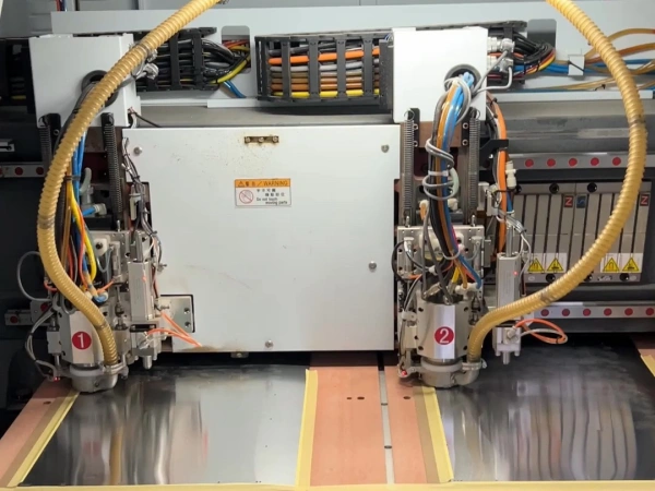
For many years in PCB making, mechanical drilling uses tungsten carbide bits that spin at 150,000-300,000 RPM to make holes in copper-clad layers. It has been used because of standard work methods, medium cost (about 50,000 to 200,000 per system), and it works on many materials like FR-4 composites and metal boards. When making larger vias (>0.15mm), this way makes 800-1,200 holes per minute on 1.6mm boards.
But there are three problems that limit its future use:
Microvia Problems: For holes under 0.1mm, bit wear happens faster. Bits need to be changed every 3,000-5,000 hits instead of every 15,000+ for bigger holes.
HDI Board Problem: Making boards with 20+ layers needs 40-60 tool changes per panel.
Material Problem: Thin-core materials (<0.2mm) show 12-18% more resin smear and nail heading defects.
Laser Ablation Advancements
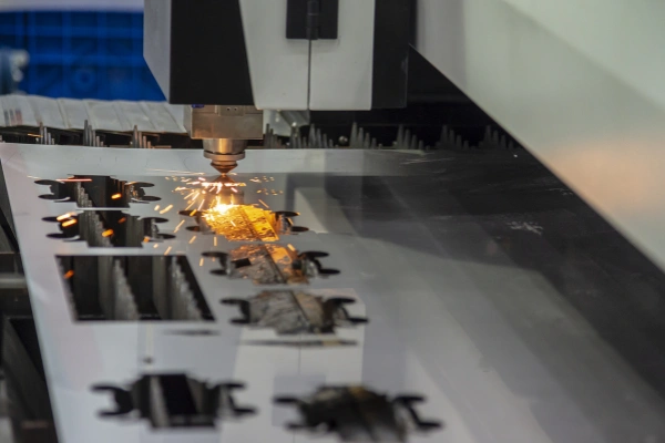
New laser systems (CO₂, UV, picosecond types) do not touch the material. They use light to break the material. They have these benefits:
The smallest via diameter is 50μm (compared to 150μm with mechanical drilling).
Position accuracy is ±5μm, which is 3 times better than mechanical.
They do not need physical tools. Cost per 1,000 laser-drilled vias is 0.15–0.30 versus 1.20–1.80 for mechanical.
Industry examples show these benefits. For example, smartphone boards now use 25μm laser-drilled microvias at 150 holes per second, and the pad size is reduced by 50% compared to mechanical methods.
Market Drivers and Technological Convergence
The rollout of 5G (needing 20-40μm annular ring widths) and the growth of flexible electronics (foldable screens that need 25μm PI substrate processing) have sped up laser use. For example:
5G AAU (Active Antenna Unit) PCBs need 0.08mm laser-drilled blind vias with less than 2% taper.
Car radar modules use 0.05mm staggered microvias made by laser to lower signal loss at 77GHz.
Some hybrid ways are now used. For example, first using mechanical pre-drilling for 0.3mm holes and then laser for 0.06mm microvias works well for server boards in terms of cost and accuracy.
Economic Analysis
UV laser systems cost 800,000–1.2M at first, while mechanical systems cost about $80,000. But overall costs change when we consider:
Yield: Laser makes scrap rates drop from 5-7% to 1.2-1.8%.
Maintenance: Annual laser upkeep is about 15,000 versus 45,000–70,000 for mechanical tools.
Throughput: Lasers work 24/7, but mechanical systems need 8-12 tool changes each day.
Break-even shows laser systems work better when making more than 15 million microvias a year. Many Tier-1 PCB makers already do this.
Material Innovation Synergy
Lasers work well with next-gen materials:
Low-loss dielectrics (Megtron 6, Tachyon-100G) let signals at 28GHz+ move through laser-made smooth via walls (Ra<1.5μm versus 3.5-4μm with mechanical).
Embedded component boards let lasers ablate cavities with ±8μm accuracy.
For ceramic substrates, UV lasers make 0.07mm vias in 96% alumina with less than 5μm chipping.
Industrial Implementation Roadmap
Current market shows:
Mechanical methods are used for 68% of through-holes and 92% of holes larger than 0.2mm in 2024.
Laser methods are used for 85% of HDI microvias and 40% of blind or buried vias in 2024.
Projections say that by 2028, laser use will increase because of:A 30% yearly drop in picosecond laser costs,
ISO 14001 rules on tungsten disposal, and
5G-Advanced rules needing holes smaller than 0.06mm.
Table of Contents
Related Posts
PCBA Prototype
April 14, 2026


