PCB Bending and Warping Causes and Solutions by PCB Factory and PCBA Suppliers
By PCBA PrototypePublished On: 2026-01-25Categories: Blog, PCBA, Services0 Comments on PCB Bending and Warping Causes and Solutions by PCB Factory and PCBA Suppliers
By PCBA PrototypePublished On: 2026-01-25Categories: Blog, PCBA, Services0 Comments on PCB Bending and Warping Causes and Solutions by PCB Factory and PCBA Suppliers

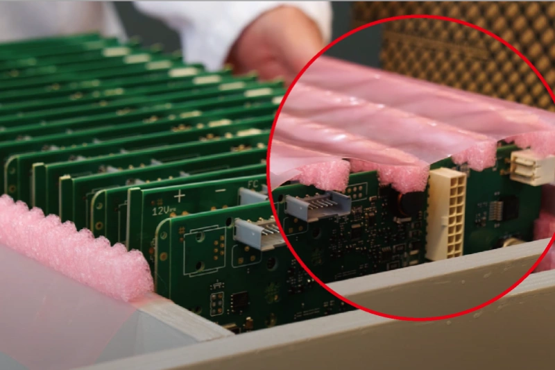
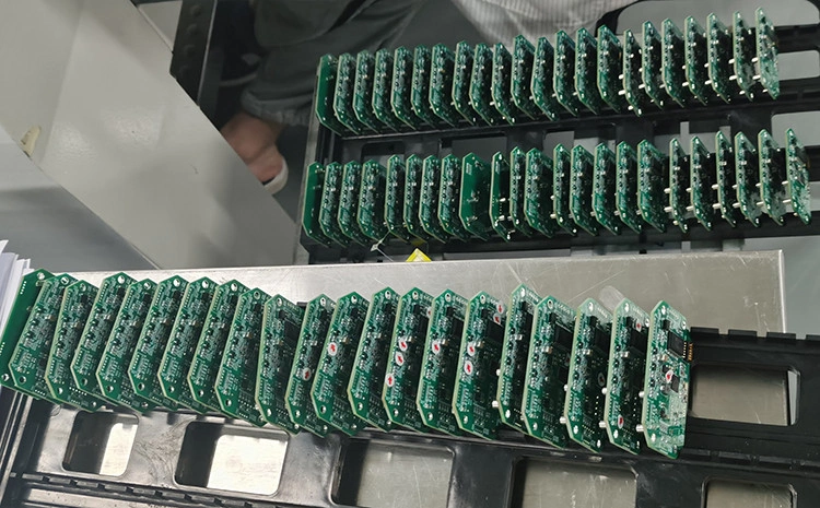
Bending or warping of PCB boards is usually caused by one or a combination of the following reasons, commonly observed in a PCB Factory environment or during handling by PCBA suppliers:
- Temperature changes: Temperature changes can cause thermal expansion or contraction of the PCB board. If both sides of the board are not subjected to the same thermal effects, it can lead to bending or warping, which is a frequent issue addressed by a PCB Factory.
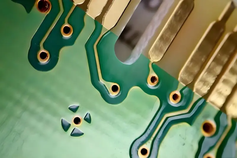
- Uneven plating: Uneven plating may result in a thicker copper layer on one side of the board and a thinner layer on the other, leading to board deformation during processing in the PCB Factory or assembly by PCBA suppliers.
- Uneven PCB board thickness: If the thickness of the PCB board is uneven, it may lead to bending or warping. This may be due to material variations during production or pressure variations on the board in the PCB Factory.
- Improper board dimensions: If the dimensions of the PCB board are incorrect, it may lead to bending or warping. This may be due to errors in the design or manufacturing process handled by the PCB Factory or communicated to PCBA suppliers.
- Uneven soldering: If the components on the board are soldered unevenly, it may lead to bending or warping. This may be due to errors in manufacturing or problems during the assembly process by PCBA suppliers.
- Poor board quality: Low-quality board materials may lead to bending or warping. This may be due to material defects or quality problems during the production process in the PCB Factory.
- Improper PCB board processing: If there are significant errors in the board processing process, it may lead to bending or warping. This may be due to errors in the processing process or machine malfunctions in the PCB Factory.
- PCB board material problems: The materials used for the PCB board may not be suitable for manufacturing requirements in a PCB Factory, which may lead to bending or warping.
- PCB board design problems: Design problems may lead to bending or warping. This may be due to the designer not considering certain factors or errors in the design process before manufacturing in the PCB Factory or assembly by PCBA suppliers.
- Mechanical stress: During transportation, installation, or use, mechanical stress may cause bending or warping of the PCB board, often reported by PCBA suppliers after delivery.
Bending or warping of PCB boards
To avoid bending or warping of PCB boards, the following measures should be taken by a PCB Factory and coordinated with PCBA suppliers:
- Select appropriate board thickness and dimensions: When designing PCBs, the appropriate board thickness and dimensions should be selected according to actual needs to ensure that the board can withstand the expected load and will not experience excessive bending or warping during processing in the PCB Factory.
- Pay attention to plating uniformity: During the PCB manufacturing process, ensure uniform plating in the PCB Factory to avoid problems such as the copper layer being too thick on one side of the board and too thin on the other, which can lead to board bending or warping.
- Control processing errors: During the PCB processing, strictly control errors in the PCB Factory to ensure that the size and shape of the board meet the design requirements, avoiding excessive bending or warping.
- Arrange components reasonably: During the PCB design and assembly process, reasonably arrange the position and spacing of components to avoid uneven distribution of components on the board, which can lead to bending or warping during assembly by PCBA suppliers.
- Control welding temperature and time: During the PCB welding process, control the welding temperature and time to avoid overheating or prolonged heating, which can cause board bending or warping, especially for PCBA suppliers.
- Pay attention to temperature changes: During the use and storage of PCBs, pay attention to temperature changes to avoid the board being affected by heat from different sides, leading to bending or warping, as recommended by PCB Factory guidelines.
- Add support structures: During the PCB design and assembly process, support structures can be added to enhance the rigidity of the board and prevent bending or warping, a common suggestion from PCBA suppliers.
- Add frames or borders: During the PCB design and assembly process, frames or borders can be added to enhance the stability and rigidity of the board and prevent bending or warping during handling in the PCB Factory and by PCBA suppliers.
In summary, PCB bending or warping is caused by a combination of factors. To avoid this problem, corresponding measures need to be taken in various aspects of PCB design, manufacturing, assembly, and use. Both the PCB Factory and PCBA suppliers must strictly control quality and errors at each stage to ensure the quality and stability of the board.
Table of Contents

Tags
Related Posts
PCBA Prototype
July 17, 2026