An In-Depth Look at the Reflow Soldering Process

Reflow soldering is a key process in the electronics industry, primarily used to attach surface-mount components to printed circuit boards (PCBs). It involves applying solder paste at specific locations on the PCB, placing components onto the paste, and then heating the assembly in a reflow oven. The solder paste melts to form a reliable electrical and mechanical connection between the components and the PCB. The quality of these connections has a significant impact on the performance and reliability of the final electronic product.
During the reflow soldering process, several factors affect solder joint quality, including the composition of the solder paste, the type of reflow oven, and the temperature profile. Understanding these factors and how they interact is crucial for achieving optimal soldering results. This article takes an in-depth look at the reflow process, discussing its various aspects, challenges, and best practices. It provides a comprehensive understanding of the techniques and principles involved, enabling readers to make informed decisions when using reflow soldering.
Reflow Soldering Process Overview
Preparing the PCB
Before reflow soldering, it’s absolutely critical to thoroughly and properly clean the PCB. The cleanliness of the PCB surface directly affects the solder paste’s ability to adhere and form reliable bonds. Dust, grease, and oxidation can lead to soldering defects and compromise product reliability.
There are various methods to clean the PCB prior to reflow, including ultrasonic cleaning, water-based cleaning, and solvent cleaning. Ultrasonic cleaning uses high-frequency sound waves to remove contaminants, while water-based cleaning relies on water-based solutions, and solvent cleaning uses specialized chemicals to dissolve contaminants. Each method has its own pros and cons depending on the type and extent of contamination, PCB material, and environmental considerations.
After cleaning, the next step is to apply the solder paste. Solder paste is a mixture of metal alloy particles, flux, and other additives that melt during the reflow process to form bonds between the PCB pads and component leads. A key aspect of solder paste application is depositing it accurately onto the PCB pads, usually accomplished with a stencil printer.
Stencil Printing
Stencil printing is a critical step in the reflow soldering process because it ensures that solder paste is accurately deposited onto the PCB pads. A well-designed stencil is essential for achieving optimal solder joint quality. Typically made from stainless steel or polyimide film, the stencil features apertures that match the layout of the PCB pads. The stencil is placed on the PCB, and a squeegee is used to spread the solder paste over the stencil, filling the apertures and transferring the paste onto the pads.
Several factors influence the quality of stencil printing and solder paste deposition:
Stencil Design: The thickness and aperture size of the stencil must precisely match the PCB pad dimensions and component requirements. The stencil’s thickness determines the amount of solder paste deposited, while the aperture size controls the lateral spread of the paste. A well-designed stencil minimizes the risk of solder bridging or insufficient solder on the pads.
Printing Parameters: The angle, pressure, and speed of the squeegee play an important role. An incorrect squeegee angle might result in incomplete filling of the apertures, while too much pressure or speed can cause smearing or misalignment of the paste. Proper calibration and adjustment of these parameters are essential.
Solder Paste Characteristics: The rheological properties of the solder paste—such as viscosity and thixotropy—affect its ability to flow through the stencil apertures and adhere to the PCB pads. The paste must have the right viscosity and thixotropic behavior to achieve consistent and accurate deposition. Key factors include metal content, alloy composition, and particle size distribution, all of which influence the final solder joint quality.
Regular inspection and maintenance of the stencil printer are crucial to prevent defects and ensure high-quality solder paste deposition. This includes cleaning the stencil to remove paste residues and verifying alignment and accuracy during the printing process.
Pick and Place
The pick-and-place process is vital during reflow soldering, where surface-mount components are precisely positioned onto the solder-paste-coated PCB pads. Pick-and-place machines (also known as component placement systems) handle this task. These machines use cameras, robotic arms, and vacuum nozzles to pick up components from reels or trays and place them accurately onto the PCB.
Several factors contribute to the efficiency and accuracy of the pick-and-place process:
Component Recognition and Positioning: Modern placement machines use advanced vision systems to identify components, determine their orientation, and ensure they are correctly aligned with the PCB pads. This is critical for preventing tombstoning, tilting, or misalignment errors.
Placement Speed: The speed at which components are picked up and placed onto the PCB directly impacts production throughput. High-speed machines can place tens of thousands of components per hour, while more versatile machines may have a lower placement rate but support a wider variety of component types and sizes.
Machine Accuracy and Repeatability: The precision of the pick-and-place machine determines the accuracy of component placement on the PCB. High-precision machines can place components within a few microns of the target location, ensuring reliable solder joints and minimizing defects during reflow. Repeatability—the machine’s ability to consistently place components within a specified tolerance—is key to maintaining high solder joint quality across multiple PCB assemblies.
Feeder Capacity and Changeover Time: The number of feeders a machine can accommodate directly affects its versatility and productivity. Machines with more feeders can handle a variety of components, reducing the need for frequent changeovers. Fast changeover times also minimize production downtime and improve overall efficiency.
Proper calibration and maintenance of the pick-and-place machine are essential for ensuring accurate component placement and minimizing defects during reflow.
Reflow Oven
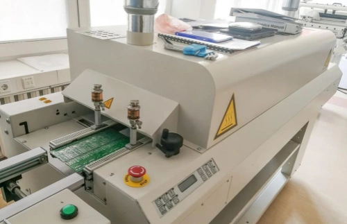
Once assembled, the PCB is transferred to the reflow oven, which is used to heat the solder paste and establish a strong bond between the surface-mounted components and the PCB. Reflow ovens use controlled temperature profiles to achieve optimal solder joint quality and reliability. The reflow process typically consists of four main stages: preheating, soaking, reflow, and cooling. Each stage is critical for forming high-quality solder joints and preventing defects related to solder.
- Preheat Stage: The PCB is gradually heated to prevent thermal shock and damage to sensitive components.
- Soak Stage: The PCB is held at a uniform temperature to activate the flux in the solder paste and remove oxides from the surfaces.
- Reflow Stage: The oven reaches peak temperatures, causing the solder paste to melt and form strong metallurgical bonds between component leads and PCB pads. For lead-free (Sn/Ag) solder, the reflow temperature range is typically 240–250°C.
- Cooling Stage: The PCB is rapidly cooled to solidify the solder joints and prevent the formation of intermetallic compounds that might weaken the connections.
Types of Reflow Ovens
There are various types of reflow ovens on the market, each with its own pros and cons. The two main types are Infrared (IR) ovens and Convection ovens.
Infrared (IR) Reflow Ovens: These use infrared radiation to heat the PCB components directly. This efficient method quickly transfers energy to the solder paste and components but can sometimes result in uneven heating due to differing material absorption characteristics. IR ovens are generally less expensive but are less common in modern electronics manufacturing due to potential heating inconsistencies.
Convection Ovens: These use heated air to transfer heat to the PCB components. Convection ovens can be further divided into two subtypes: forced-air convection and vapor-phase reflow ovens. Forced-air ovens use fans to circulate hot air around the PCB, providing uniform heating and minimizing temperature variations. Vapor-phase reflow ovens use a heat transfer medium (such as a high-boiling-point liquid) to evenly heat the PCB as the liquid evaporates, offering highly controlled and uniform heating. Although convection ovens tend to be more expensive than IR ovens, they provide superior temperature control and even heating, making them the preferred choice in modern electronics manufacturing.
The choice of a reflow oven depends on factors such as production volume, budget, and specific process requirements. Proper calibration and maintenance of the reflow oven are essential to ensure optimal solder joint quality and minimize defects related to soldering.
Reflow Oven Zones
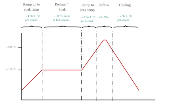
Typical Reflow Oven Temperature Profile
A typical reflow oven is divided into several zones, each with independently controlled temperature settings. The layout of these zones is crucial for achieving precise and uniform temperature distribution throughout the reflow process. Common zones include:
- Preheat Zone: Gradually raises the temperature of the PCB assembly to prevent thermal shock. The temperature ramp rate here is critical; heating too quickly can deform components, while heating too slowly might dry out the solder paste. An ideal preheat rate is about 1–3°C per second.
- Soak Zone: Maintains a constant temperature, allowing the PCB to reach a uniform temperature. This stage is vital for activating the flux in the solder paste and removing oxides from the surfaces.
- Reflow Zone: The area where peak temperature is reached, causing the solder paste to melt and form strong metallurgical bonds. The peak temperature usually ranges between 235°C and 250°C, depending on the solder paste used. Maintaining the temperature within this range for the correct duration is critical.
- Cooling Zone: Rapidly cools the assembly to solidify the solder joints. A controlled cooling rate is important to prevent the formation of brittle intermetallic compounds. An ideal cooling rate is about 2–4°C per second.
More advanced reflow ovens may feature additional zones or sub-zones for fine-tuning the temperature profile, further enhancing process control and ensuring consistent solder joint quality.
Temperature Profile
The temperature profile is a key aspect of the reflow process because it influences solder joint quality and reliability. It represents the temperature changes that the PCB assembly undergoes throughout the reflow oven. An optimal temperature profile is essential for achieving ideal solder joints while minimizing defects.
- Ramp-Soak-Spike (RSS) Profile: In the RSS profile, the temperature gradually increases in the preheat zone, holds steady in the soak zone, and then spikes to peak in the reflow zone before cooling down. This profile ensures that the PCB assembly experiences controlled temperature changes, preventing thermal shock and reducing defects like solder bridging and voids.
- Ramp-to-Spike (RTS) Profile: The RTS profile involves a continuous temperature rise from the preheat zone to the reflow zone without a distinct soak phase. This profile is often used in lead-free soldering processes, allowing for a faster heating rate to accommodate the higher melting point of lead-free solder alloys.
- Custom Temperature Profiles: Depending on the specific requirements of the PCB assembly and the solder paste used, custom profiles can be developed. Factors such as PCB complexity, component density, component types, and the thermal properties of the solder paste influence the selection of a custom profile. Custom profiles allow for precise control of the reflow process, optimizing solder joint quality and minimizing defects.
To achieve the desired temperature distribution, the reflow oven must be precisely calibrated, and its heating elements adjusted accordingly. Regular thermal analysis is recommended to ensure that the oven maintains its performance and provides consistent solder joint quality. Thermal analysis involves using thermocouples or specialized analysis boards attached to the PCB to measure the temperature at various points throughout the reflow process. The data collected can then be used to fine-tune the oven settings and optimize the temperature profile.
Solder Paste
Solder paste is a critical material in the reflow soldering process as it forms the electrical and mechanical connection between the components and the PCB. It consists of tiny solder alloy particles suspended in a flux medium, which helps clean the surfaces to be soldered, improve wetting, and prevent oxidation during the soldering process.
Components of Solder Paste
Solder paste primarily contains two main components: the solder alloy and the flux. The specific composition of the solder paste depends on the application requirements and the type of solder alloy used.
- Solder Alloy: The solder alloy is made up of tiny metal particles, typically ranging from 20–50 microns in diameter. The alloy’s composition determines the melting point, wetting properties, and mechanical strength of the solder joints. Common solder alloys include tin-lead (SnPb) and lead-free alternatives such as tin-silver-copper (SAC).
- Flux: Flux is a chemically active medium that surrounds the solder particles and plays several roles during reflow. It helps remove any oxides from the surfaces to be soldered, promotes solder wetting, and prevents further oxidation during the soldering process. Flux can be categorized into low, medium, and high activity levels based on its effectiveness. The choice of flux depends on the degree of oxidation on the surfaces, the solder alloy type, and the desired solder joint quality.
In addition to these primary components, solder paste may also contain additives such as rheology modifiers to improve printability and stability, as well as surfactants to enhance wetting properties. The specific formulation of the solder paste must be customized to meet the requirements of the reflow soldering process, taking into account factors such as component types, PCB materials, and the thermal distribution in the reflow oven.
Choosing the Right Solder Paste
Selecting the appropriate solder paste for a specific application is critical for achieving optimal soldering performance, high yield, and long-term reliability. Several factors must be considered:
- Type of Solder Alloy: The choice of solder alloy is a key factor. Tin-lead (SnPb) alloys are widely used in the electronics industry due to their excellent solderability, low cost, and ease of use. However, environmental concerns and regulations have driven the adoption of lead-free alloys such as SAC, which have higher melting points and different wetting properties.
- Flux Activity Level: The flux’s activity level in the solder paste should be chosen based on the oxidation level of the surfaces and the required solder joint quality. For highly oxidized surfaces or critical applications requiring high joint quality, a higher activity flux might be needed. Conversely, a lower activity flux might suffice for clean surfaces.
- Particle Size Distribution: The particle size distribution of the solder alloy affects the paste’s printability, reflow performance, and void formation. Smaller particles typically provide better printability and reduce voids, but they may also be more prone to oxidation and handling issues. Common particle size distributions include Type 3 (25–45 microns) and Type 4 (20–38 microns).
- Viscosity and Rheology: The solder paste’s viscosity and rheological properties must be compatible with the stencil printing process and equipment. For consistent and precise deposition on the PCB, the paste must exhibit proper flow and thixotropic behavior.
- Thermal Stability: The solder paste must have sufficient thermal stability to withstand the reflow process’s temperature profile, which includes preventing premature flux activation, solder ball formation, and slump.
- Compatibility with Components and PCB Materials: The paste should be compatible with the materials used in the components and PCBs, as well as any surface finishes, to avoid issues such as dewetting, solder joint embrittlement, and intermetallic compound formation.
For best performance, it’s essential to evaluate and test the selected solder paste under actual production conditions—including stencil printing, component placement, and reflow soldering. This helps identify potential issues and fine-tune process parameters for optimal results.
Challenges in the Reflow Soldering Process and Solutions
Tombstoning
Tombstoning (also known as the Manhattan effect) is a common soldering defect that occurs when a surface-mount component, typically a chip resistor or capacitor, lifts from one end and stands vertically on the PCB. This defect can result in open circuits and potential failure of the electronic assembly.
Causes of Tombstoning:
- Uneven Heating: If one side of a component reaches the solder’s melting point faster than the other, the surface tension of the molten solder can pull the component into a vertical position. Ensuring even temperature distribution in the reflow oven according to the solder paste and component specifications can help alleviate this issue.
- Uneven Wetting: Differences in wetting rates between the two ends of the component can also cause tombstoning. Factors include the geometry of the component and pad, solder paste composition, and PCB surface finish. Optimizing stencil design, selecting the right solder paste, and ensuring consistent PCB surface quality are key to resolving this.
- Misalignment of Components and Pads: Poor alignment can result in uneven solder distribution, increasing the risk of tombstoning. Accurate component placement and proper pad design are essential for reducing this defect.
- Component and Pad Size: Using components with larger bodies or wider terminations can help improve stability during reflow, reducing the risk of tombstoning. Ensuring that pad sizes are compatible with the selected components also helps maintain balanced solder distribution.
Implementing robust quality assurance, monitoring the reflow process, and adjusting parameters based on feedback can significantly reduce the occurrence of tombstoning and improve overall assembly reliability.
Voids
Voids are pockets of gas or air trapped within the solder joint during reflow. They can adversely affect the electrical and thermal performance of the joint, leading to reduced reliability and potential failures, particularly in BGA or QFN packages.
Causes of Voids:
- Outgassing: Gas generated during reflow from the solder paste or the component itself can become trapped if there isn’t adequate venting or if the solder paste viscosity is too high.
- Oxidation: The presence of oxides on component leads, pads, or solder balls can hinder proper wetting, leading to void formation. Proper storage and handling of solder paste and components can help minimize oxidation-related voids.
- Solder Paste Handling and Storage: Improper handling or storage—such as exposure to humidity or temperature fluctuations—can alter the solder paste’s viscosity and consistency, leading to voids. Following manufacturer guidelines for storage is essential.
Solutions to Reduce Voids:
- Optimize Reflow Temperature Profile: Adjust the temperature ramp so that the solder paste gradually reaches the melting point, allowing sufficient time for gases to escape.
- Solder Paste Selection: Choose a solder paste formulated to minimize voids, with an appropriate flux chemistry and viscosity.
- Stencil Design and Printing: Ensure that the stencil is designed correctly with proper aperture dimensions and that the solder paste is applied consistently to promote uniform deposition.
- Component and PCB Preparation: Ensure that both components and PCB surfaces are free of contaminants and oxidation to improve wetting and reduce the likelihood of voids forming.
By understanding and controlling the factors that lead to voids, manufacturers can effectively reduce their occurrence, resulting in more reliable and robust electronic assemblies.
Solder Balls
Solder balls refer to the small, unintended balls of solder that can form during the reflow process. These can cause electrical shorts, reduce joint strength, and compromise the reliability of the electronic assembly.
Causes of Solder Balls:
- Flux Activity in the Solder Paste: While flux is crucial for reducing oxides, overly active or insufficiently viscous flux can cause the molten solder to separate and form isolated balls.
- Oxidation of Solder Particles: Oxidation on the surface of solder particles can hinder coalescence during reflow, leading to the formation of solder balls. Proper storage and handling can help minimize oxidation.
- Solder Paste Printing Accuracy: Misalignment or inconsistent solder paste deposition can lead to solder ball formation during reflow. Accurate stencil printing and proper stencil design are essential.
- Reflow Temperature Profile: An inappropriate reflow temperature curve can cause the solder paste to melt too quickly or not fully coalesce, resulting in solder balls.
Solutions for Solder Balls:
- Solder Paste Selection: Use solder paste with the right flux activity and viscosity to help prevent solder ball formation. Consult with solder paste suppliers for recommendations tailored to your application.
- Optimize Reflow Temperature Profile: Adjust the temperature curve to ensure a gradual ramp-up and sufficient time above the solder’s melting point to promote proper coalescence.
- Stencil Design and Printing: Ensure the stencil is designed correctly, with consistent aperture dimensions, to enable uniform solder paste deposition.
- Component and PCB Surface Treatment: Keeping surfaces clean and oxide-free improves wetting and coalescence, reducing the likelihood of solder ball formation. Proper handling, storage, and cleaning procedures are vital.
By addressing the factors that contribute to solder ball formation and implementing appropriate process controls, manufacturers can significantly reduce this defect and enhance the reliability of their electronic assemblies.
Inspection and Quality Control
Visual Inspection
Visual inspection is a critical step in ensuring the quality of surface-mount soldering. It involves checking the solder joints and components on the PCB for any defects or irregularities that might affect the performance and reliability of the assembled device. Visual inspection can be performed manually or with the help of Automatic Optical Inspection (AOI) systems.
Manual Visual Inspection: This involves operators closely examining the PCB under magnification to identify potential defects. While manual inspection allows for human judgment in determining whether a solder joint is acceptable or requires rework, it can be time-consuming and prone to human error. Skilled operators are needed to ensure consistent and accurate results.
Automatic Optical Inspection (AOI): AOI systems use cameras, lighting, and image processing software to automatically inspect PCBs for defects by comparing captured images against predefined standards. AOI offers advantages in speed, accuracy, and repeatability compared to manual inspection. These systems can detect a variety of defects, including solder bridges, misaligned components, and insufficient solder.
Defect Detection:
The goal of visual inspection, whether manual or automated, is to identify various soldering defects such as:
- Solder Bridges: Unintended connections between adjacent solder joints that could cause short circuits.
- Insufficient Solder: Not enough solder in a joint, leading to weak mechanical and electrical connections.
- Excessive Solder: Too much solder, which can cause shorts or affect the performance of nearby components.
- Misaligned Components: Incorrectly placed components that could result in poor electrical connections or mechanical stress.
Post-Inspection Measures:
After inspection, any detected defects must be addressed. This may involve rework processes, such as desoldering and resoldering components or removing excess solder. Recording inspection results and any subsequent rework is crucial for traceability and improving process control.
X-Ray Inspection
X-ray inspection is a non-destructive testing method used to evaluate solder joint quality and detect hidden defects in surface-mount assemblies. This technique is particularly useful for examining solder joints that are not visible optically, such as those under Ball Grid Array (BGA) or Quad Flat No-Lead (QFN) packages.
X-Ray Inspection Process:
An X-ray system generates X-rays that pass through the PCB and are captured by a detector to produce radiographic images of the internal structure of the solder joints. The contrast in the images is determined by the differing X-ray absorption of materials—denser materials like metals appear brighter. Operators or automated software then analyze these images to identify potential defects.
Defects Detected by X-Ray Inspection:
X-ray inspection is effective at identifying defects that are difficult or impossible to see through visual methods, including:
- Voids: Gas pockets or gaps within the solder joint that can weaken its mechanical and thermal properties.
- Bridging: Unintended solder bridges beneath surface-mount components.
- Insufficient or Excessive Solder: Hidden solder volume issues that could affect joint performance.
Limitations of X-Ray Inspection:
While powerful, X-ray inspection does have limitations:
- False Positives/Negatives: Misinterpretation of X-ray images can lead to false identification of defects. Careful analysis and correlation with other inspection methods help mitigate this risk.
- Material Limitations: X-ray inspection may be less effective when materials have similar X-ray absorption characteristics, making differentiation difficult.
X-ray inspection should be integrated with other methods, such as visual inspection and AOI, to ensure comprehensive defect detection and quality control. Combining multiple inspection techniques allows manufacturers to more effectively identify and address potential issues, thereby improving overall product reliability and performance.
Automatic Optical Inspection (AOI)
AOI is a non-contact, high-speed inspection method widely used in electronics manufacturing to ensure the quality of PCB assemblies. AOI systems utilize cameras and image processing software to automatically inspect PCBs, comparing captured images against predefined standards to identify any defects or deviations from the reference design.
Key Components of an AOI System:
- High-Resolution Cameras: These capture detailed images of the PCB surface from multiple angles, increasing the likelihood of detecting defects.
- Lighting: Consistent and uniform lighting is crucial for accurate image capture. AOI systems typically use multiple light sources with various wavelengths and angles to achieve the necessary contrast and minimize shadows.
- Image Processing Software: This software processes the images and compares them with reference data to identify potential defects. Advanced AOI systems use machine learning algorithms to improve detection accuracy and adapt to variations in component appearance and solder joint quality.
Defect Detection by AOI:
AOI systems can detect a variety of defects, including:
- Component Presence, Orientation, and Alignment: Ensuring all components are present, correctly oriented, and accurately placed on their respective pads.
- Solder Joint Quality: Analyzing the shape, size, and color of solder joints to identify issues such as insufficient or excessive solder, bridging, and poor wetting.
- Component Polarity: Verifying that components with polarity requirements are installed correctly to prevent potential failures or damage.
Speed and Accuracy:
One of the main advantages of AOI is its speed—capable of inspecting thousands of components per hour, far surpassing manual methods. The accuracy of AOI systems depends on camera resolution, lighting conditions, and the sophistication of the image processing algorithms. Typical systems can achieve a defect detection rate of 90% or higher, with a false-positive rate below 10%.
Limitations of AOI:
While AOI is a powerful tool, it does have limitations:
- Hidden Solder Joints: AOI cannot inspect solder joints that are hidden from optical access, such as those under BGAs or QFN packages. X-ray inspection is required for these.
- Component Appearance Variations: Variations in component appearance due to manufacturing tolerances or supplier changes can challenge AOI systems, potentially leading to false positives or missed defects. Regular calibration and operator training help mitigate these issues.
- Integration with Other Methods: AOI should be part of a comprehensive inspection strategy that includes visual, X-ray, and functional testing to ensure overall quality and reliability.
Conclusion
In the electronics manufacturing industry, the reflow soldering process is crucial for ensuring reliable, high-quality PCB assemblies. By understanding the principles of reflow soldering, manufacturers can optimize their processes for consistent, high-quality results. Addressing challenges such as tombstoning, voids, and solder balls requires a thorough understanding of their root causes and the implementation of appropriate corrective measures. Inspection and quality control techniques, including visual inspection, X-ray inspection, and AOI, are vital for verifying solder joint quality and identifying potential issues before they affect the final product’s performance. By integrating these concepts and methods, manufacturers can improve efficiency, yield, and overall product reliability in their electronics manufacturing processes.
Related Posts
PCBA Prototype
December 14, 2025
PCB Assembly
September 2, 2025


