Co-evolution of SiP and PCB Design
Abstract
This article delves into the synergistic development of ultra-high-density packaging (SiP) and PCB design. It elaborates on the significance of their integration, explores the challenges and solutions in the process, and showcases successful application cases. By analyzing the trends and prospects, it highlights the crucial role this synergy plays in the advancement of modern electronics, aiming to provide valuable insights for professionals in related fields.
1. Introduction
1.1 Background
In recent years, the electronics industry has witnessed a remarkable trend towards miniaturization and multifunctionality. With the continuous advancement of technologies such as the Internet of Things (IoT), 5G communication, wearable devices, and artificial intelligence, consumers demand more compact, powerful, and feature-rich electronic products. This has led to a significant increase in the complexity of electronic systems, posing new challenges to traditional printed circuit board (PCB) design and packaging technologies.

Ultra-high-density packaging, especially System-in-Package (SiP), has emerged as a crucial solution to meet these demands. SiP integrates multiple chips, passive components, and even microelectromechanical systems (MEMS) into a single package, achieving a high level of functional integration. It enables shorter interconnections between components, reduces signal propagation delays, and improves overall system performance. However, the successful implementation of SiP heavily relies on seamless cooperation with PCB design. The PCB serves as the foundation for mounting and interconnecting various components, and its design needs to be optimized in conjunction with SiP to fully realize the advantages of high-density packaging.
1.2 Purpose
This article aims to explore the synergistic development of SiP and PCB design. By analyzing the current state of the art, challenges, and solutions in this field, we hope to provide valuable insights for professionals in the electronics manufacturing industry. Understanding the relationship between SiP and PCB design and how they can work together to overcome technical hurdles is essential for driving innovation and improving the competitiveness of electronic products. We will also showcase some successful application cases and discuss future trends, with the goal of inspiring further research and development efforts to promote the continuous evolution of this critical aspect of electronics manufacturing.
2. Understanding SiP Technology
2.1 Definition and Architecture
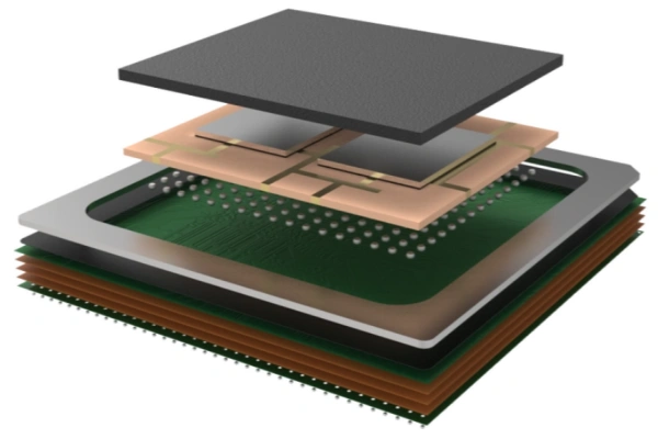
According to the definition provided by the International Technology Roadmap for Semiconductors (ITRS), System-in-Package (SiP) refers to the integration of multiple active electronic components with different functions, along with optional passive devices, and other components such as microelectromechanical systems (MEMS) or optical devices, into a single standard package to form a system or subsystem. Architecturally, SiP combines various functional chips, including processors, memories, and other components, within one package to achieve a substantially complete functionality.
In contrast to System-on-Chip (SoC), which integrates all necessary components onto a single die through design, SiP takes a different approach. It allows for the combination of chips fabricated using different processes and technologies. For example, a SiP module might incorporate a high-performance processor chip, fabricated with advanced CMOS technology to ensure computational power, along with a specialized memory chip optimized for data storage and retrieval. These chips can be arranged either side by side or stacked, depending on the specific requirements of the application. This flexibility in architecture enables SiP to overcome some of the limitations faced by SoC, especially in terms of integrating heterogeneous components and accommodating different manufacturing processes.

2.2 Advantages of SiP
One of the most significant advantages of SiP is its shorter development cycle. Unlike SoC, which requires extensive design and verification efforts for each integrated component, SiP leverages existing, pre-verified chips. This means that manufacturers can quickly assemble and package the required components to meet market demands in a timely manner. For instance, in the fast-paced consumer electronics market, where product lifecycles are short and new features need to be introduced rapidly, SiP allows companies to bring innovative products to market within months rather than years.
SiP also offers enhanced functional integration. By combining multiple chips and passive components, it can provide a comprehensive set of functions within a compact package. Consider a wearable health monitoring device. A SiP module can integrate a microcontroller for data processing, a sensor for monitoring vital signs such as heart rate and blood pressure, and a wireless communication chip for transmitting the data to a smartphone or cloud server. This level of integration not only saves space but also improves the overall performance and reliability of the system.
Moreover, SiP can contribute to lower power consumption. With shorter interconnections between components compared to traditional PCB-based designs, signal propagation delays are reduced, and power losses during transmission are minimized. In battery-powered devices like smartphones, smartwatches, and IoT sensors, this can significantly extend the battery life, enhancing the user experience and reducing the need for frequent recharging.
2.3 SiP Packaging Processes
SiP packaging primarily employs two main processes: wire bonding and flip-chip bonding.
Wire bonding is a well-established and widely used technique. The process begins with wafer thinning, where the thickness of the wafer is reduced from its original value to an appropriate level for packaging. This is typically achieved through mechanical or chemical mechanical polishing (CMP). Subsequently, the wafer is cut into individual chips using precision sawing or laser cutting techniques. Once the chips are obtained, they are bonded onto the substrate. The bonding material can vary, including soft solders like Pb-Sn alloys or Au-Si eutectic alloys, or polymer adhesives in the case of plastic packaging. After chip bonding, fine wires, usually made of gold, are used to establish electrical connections between the chip pads and the substrate pads. The wire diameter is typically in the range of 0.025mm to 0.032mm, and the length and arc height are carefully controlled to ensure reliable connections. Keybonding technologies include thermocompression bonding and thermosonic bonding, each with its own advantages in terms of bond formation and temperature control.

#image_title
Flip-chip bonding, on the other hand, offers several advantages in terms of higher interconnect density and better electrical performance. In this process, the chips are flipped upside down, and solder bumps are formed on the chip pads. These bumps are then aligned and reflowed to create direct electrical connections with the corresponding pads on the substrate. Before the flip-chip process, the wafer often undergoes additional processing steps, such as redistribution layer (RDL) formation to optimize the chip’s I/O layout. The solder bump materials and sizes are carefully selected to ensure reliable mechanical and electrical connections. Compared to wire bonding, flip-chip bonding reduces the length of the interconnects, leading to lower parasitic inductance and capacitance, which is crucial for high-speed digital and RF applications.
3. PCB Design Essentials
3.1 Layers and Their Functions
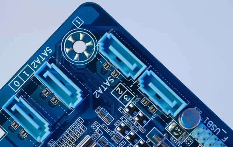
A typical PCB consists of multiple layers, each serving a specific purpose. The signal layers are primarily responsible for routing the electrical signals between components. These layers are carefully designed to minimize signal interference and ensure proper signal integrity. For example, in high-speed digital circuits, impedance-controlled traces are often used on the signal layers to match the impedance of the connected components, reducing signal reflections and maintaining the quality of the transmitted signals.
The power and ground planes play a crucial role in providing stable power distribution and a low-impedance return path for the signals. They help reduce power supply noise and electromagnetic interference (EMI). In multilayer PCBs, dedicated internal power and ground planes are used to distribute power evenly across the board. For instance, in a motherboard for a desktop computer, multiple power planes might be used to supply different voltages to various components such as the CPU, graphics card, and memory modules, while the ground plane provides a common reference for all signals.
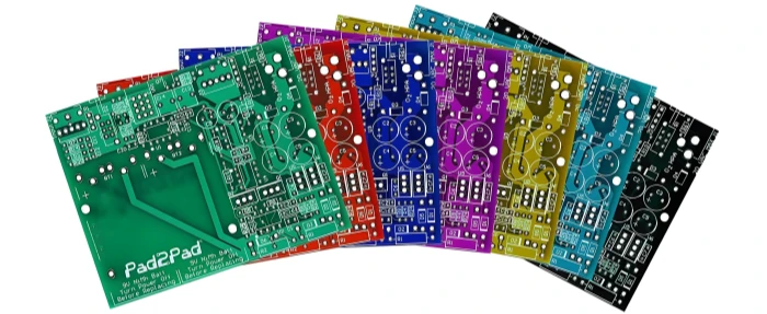
The solder mask layer is applied to protect the copper traces on the PCB and prevent short circuits by covering areas that should not be soldered. It also helps in defining the solderable areas for components. The silk screen layer, on the other hand, contains markings, component designators, and other reference information that assist in the assembly and debugging processes. It allows technicians to easily identify the location and orientation of each component during manufacturing and maintenance.
3.2 Design Considerations
In the layout phase, components need to be arranged strategically. High-power components should be placed away from sensitive ones to avoid heat and electrical interference. For example, in a power amplifier circuit, the power transistors generating significant heat are positioned at a distance from the low-noise amplifier stages to prevent thermal noise from degrading the signal quality. Grouping related components together also simplifies wiring and improves overall circuit performance. In a microcontroller-based system, the microcontroller, its associated passive components like capacitors and resistors, and the connectors for external interfaces are often grouped in a specific area to minimize trace lengths and signal propagation delays.
Routing involves determining the paths for the electrical connections between components. High-speed signals require careful consideration to prevent signal integrity issues such as crosstalk and impedance mismatches. Differential pairs are commonly used for high-speed data transmission, where two traces are routed closely together with controlled impedance and equal length to minimize noise pickup and maintain signal balance. Power and ground traces should be wide enough to handle the current requirements, typically with widths calculated based on the expected current load to reduce resistive losses and voltage drops.
Thermal management is essential, especially in high-power applications. Heat sinks, vias, and thermal pads can be incorporated into the PCB design to dissipate heat effectively. For example, in a graphics card PCB, large copper areas and multiple vias are used to conduct heat away from the GPU chip to the metal heat sink attached to the board. Additionally, proper airflow channels need to be considered in the overall system design to enhance heat dissipation and prevent overheating, which can lead to component failure and reduced reliability.
4. The Symbiotic Relationship
4.1 SiP’s Impact on PCB Design
4.1.1 Reducing Board Complexity
Take the example of True Wireless Stereo (TWS) earbuds. In the past, the PCB of TWS earbuds had to accommodate numerous discrete components, such as the Bluetooth chip, audio codec, power management IC, and various passive components. This led to a complex web of interconnections and a large number of solder joints, increasing the risk of manufacturing defects and signal interference. With the adoption of SiP technology, multiple chips and passive components are integrated into a single module. For instance, a SiP module for TWS earbuds can integrate the Bluetooth audio SoC, which combines the functions of Bluetooth communication, audio processing, and power management. This significantly reduces the number of components on the PCB and simplifies the circuit layout. As a result, the number of nodes that need to be connected on the PCB is greatly reduced. In some advanced TWS earbud designs, after integrating the functions into a SiP, the number of nodes on the PCB is reduced by more than 50%, from dozens to just a few key connection points. This not only shortens the production cycle but also improves the overall reliability of the product.

4.1.2 Enabling Miniaturization
SiP technology plays a crucial role in enabling the miniaturization of PCB-based products. In today’s consumer electronics market, products like smartwatches, fitness trackers, and IoT sensors are constantly evolving towards smaller form factors. The integration capabilities of SiP allow multiple functions to be concentrated in a compact package. Consider a smartwatch, which needs to integrate components such as a microprocessor, memory, sensor interface, and wireless communication module. By using SiP, these components can be stacked or arranged in a highly integrated manner within a small space. This, in turn, reduces the area occupied by the components on the PCB. For example, compared to traditional discrete component designs, the use of SiP can reduce the PCB area by 30% – 50% in some smartwatch applications. As a result, the overall size of the product can be further reduced, meeting the market demand for portability and wearability.

4.1.3 Altering Signal Integrity Requirements
The integration of components within a SiP changes the way signals are transmitted and received compared to traditional PCB designs. In a SiP, the interconnections between chips are much shorter, which can reduce signal propagation delays and parasitic effects. However, this also brings new challenges to signal integrity. For example, in high-speed digital circuits, the impedance matching requirements become more critical. Since the signals within the SiP travel over shorter distances, any impedance mismatch can lead to significant signal reflections and degradation. In addition, the close proximity of different functional blocks within the SiP can cause crosstalk issues. For RF circuits integrated in a SiP, the coupling between the antenna and other components needs to be carefully considered to ensure proper signal transmission and reception. PCB designers need to take these factors into account and use techniques such as controlled impedance routing, differential pairs, and shielding to maintain signal integrity. For instance, in a 5G mobile phone SiP module, the PCB designer needs to ensure that the impedance of the RF traces is precisely controlled within a narrow tolerance range to support high-speed data transmission.
4.2 PCB Design Adaptations for SiP
4.2.1 Layout Optimization
To accommodate SiP modules effectively, the layout of the PCB needs to be carefully optimized. Firstly, the position of the SiP module on the PCB should be determined based on its functionality and heat dissipation requirements. For example, if the SiP contains a high-power processor, it should be placed in an area with good heat dissipation, such as near a heat sink or in a position with sufficient airflow. Secondly, the layout of other components around the SiP needs to be coordinated. Related passive components, such as decoupling capacitors, should be placed as close as possible to the corresponding pins of the SiP to reduce the length of power and ground traces and minimize parasitic inductance. In a motherboard design for a desktop computer that incorporates multiple SiP modules for different functions, the layout is carefully planned to ensure that the data transmission paths between the SiP modules and other components, such as memory modules and expansion slots, are as short as possible to improve overall system performance.
4.2.2 Routing Considerations
Routing on the PCB in the presence of SiP requires special attention. The pin distribution of the SiP dictates the initial routing paths. High-speed signals need to be routed away from noisy components and power traces to avoid crosstalk. For example, in a PCB for a high-definition video processing device, the differential pairs used for transmitting video signals from the SiP to the display interface are carefully routed to maintain signal balance and integrity. The length matching of these differential pairs is crucial, typically with tolerances within a few millimeters to prevent skew. In addition, the power and ground routing for the SiP must be designed to handle the current requirements. Wide power planes and multiple vias are often used to ensure a low-impedance path for power supply, reducing voltage drops. For a SiP module in a server motherboard that consumes significant power, the power traces are designed to be several times wider than normal traces and are connected to multiple layers of power planes through vias to ensure stable power delivery.
4.2.3 Thermal Management
SiP modules, especially those with high-power components, generate a significant amount of heat. Therefore, the PCB design needs to incorporate effective thermal management measures. One common approach is to use thermal vias. These vias are filled with thermally conductive materials and connect the heat-generating components on the PCB to the ground or heat sink layers. In a graphics card PCB, dozens of thermal vias are often used around the GPU SiP module to conduct heat away. Another method is to use a thermal pad or heat spreader on the PCB. A thermal pad made of materials with high thermal conductivity, such as copper or graphite, is placed between the SiP and the PCB to enhance heat transfer. In addition, the overall PCB layout should consider the airflow direction to ensure that cool air can flow through the heat-generating areas. In a computer chassis design, the position and orientation of the PCB are optimized to cooperate with the cooling fans, allowing hot air to be exhausted efficiently and cool air to be supplied to the components that need it.

5. Future Trends
5.1 Advancements in SiP Technology
The future of SiP technology holds great promise. We can anticipate even higher levels of integration, with more diverse components being incorporated into a single package. For example, in the field of biomedical applications, SiP modules could integrate microfluidic chips for sample handling, biosensors for detecting specific biomarkers, and signal processing chips for real-time analysis. This would enable the development of compact, portable diagnostic devices with enhanced functionality.
Performance enhancements will also be a key focus. Reducing power consumption further will be crucial, especially for emerging applications such as the Internet of Things (IoT), where devices are often battery-powered and need to operate for extended periods without frequent recharging. New interconnect technologies, like silicon interposers with finer pitch and higher bandwidth, will be developed to meet the demands of high-speed data transfer. For instance, in 5G and future 6G communication systems, SiP modules with advanced interconnects will be essential to handle the massive amounts of data being transmitted and received at extremely high frequencies.
5.2 Evolution of PCB Design
PCB design will continue to evolve in tandem. Higher density designs will become the norm, with narrower trace widths and smaller vias to accommodate the increasing complexity of integrated circuits. In high-performance computing applications, such as data centers and supercomputers, PCBs will need to support extremely high-speed signals while minimizing signal loss and crosstalk. This will require the use of advanced materials with better dielectric properties and improved manufacturing processes to achieve precise impedance control.
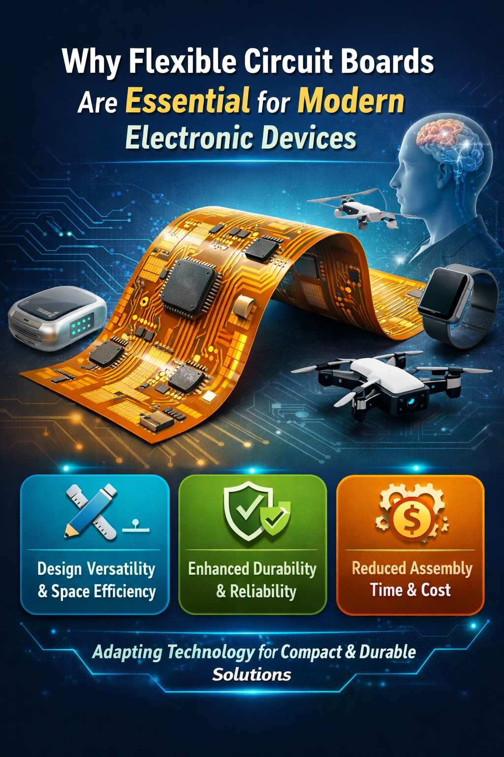
Flexible PCBs will gain more prominence, especially in wearable and flexible electronics. These PCBs can conform to different shapes and provide greater design flexibility. For example, in smart clothing or implantable medical devices, flexible PCBs can be integrated seamlessly, enabling the development of innovative products that are comfortable to wear and have minimal impact on the user’s daily activities. Additionally, the integration of passive components directly onto the PCB substrate, known as embedded passives, will reduce the overall component count and further miniaturize the PCB layout.
5.3 Continued Synergy
The continued synergy between SiP and PCB design will be the driving force behind the innovation of future electronic products. As both technologies advance, manufacturers will be able to create more sophisticated and compact systems. In the automotive industry, for example, the combination of advanced SiP modules for engine control, driver assistance systems, and infotainment, along with optimized PCB designs, will lead to smarter and more energy-efficient vehicles.
This synergy will also open up new application areas. In the field of space exploration, miniaturized satellites and spacecraft can benefit from the high-density integration of SiP and the reliable interconnect provided by PCB design. These technologies will enable the development of lightweight, high-performance space systems that can carry out complex missions with reduced costs. Overall, the collaborative development of SiP and PCB design is set to shape the future of the electronics industry, bringing about a new era of smaller, faster, and more intelligent electronic devices.
6. Conclusion
In conclusion, the synergistic development of SiP and PCB design has already achieved remarkable results. SiP technology, with its advantages of high integration, short development cycle, and low power consumption, has brought revolutionary changes to the design and manufacturing of electronic products. It has effectively addressed the challenges of miniaturization and multifunctionality in modern electronics. Meanwhile, PCB design has continuously adapted and evolved to accommodate SiP modules, optimizing layout, routing, and thermal management to fully unleash the potential of SiP.
Through successful application cases in consumer electronics, wearable devices, and other fields, we have witnessed the significant value and competitiveness that this synergy can bring. However, challenges such as signal interference, thermal issues, and design standardization still remain. Overcoming these hurdles requires continuous innovation in materials, processes, and design methodologies.
Looking ahead, the future of SiP and PCB design holds even greater promise. With advancements in SiP technology enabling higher integration and better performance, and the evolution of PCB design towards higher density and flexibility, the two will continue to work hand in hand. This continued synergy will not only drive the innovation of electronic products in existing application areas but also open up new possibilities in emerging fields. It will play a crucial role in shaping the next generation of smaller, faster, and more intelligent electronic devices, further propelling the development of the entire electronics industry. Professionals in related fields should closely monitor these trends and actively engage in research and development to stay at the forefront of this dynamic technological evolution.
Related Posts
PCBA Prototype
December 8, 2025
PCBA Prototype
November 9, 2025


