Detailed Overview of the PCBA Process

To make a bare PCB functional, components need to be mounted on it, which is the process known as PCBA. For engineers, PCBA is a fundamental skill.
Component Procurement and Storage
Before starting the PCBA process, we need to purchase components. These components generally fall into passive and active categories. Passive components include resistors, capacitors, inductors, etc. SMT components are usually sold on reels, either as a full reel or a cut reel. Active components are semiconductor devices, such as chips. It’s essential to avoid using recycled or refurbished chips, as the time cost to troubleshoot issues can far exceed the cost of purchasing genuine components. We usually keep some spare components, which must be stored properly to prevent oxidation or changes in parameters due to temperature and humidity, which can affect soldering and functionality.

SMT PCBA Manufacturing Process
The PCBA process for a circuit board typically begins with the BOM (Bill of Materials), which guides the procurement or collection of components. When performing SMT PCBA, attention must be paid to whether all components need to be mounted in a single pass for reflow soldering. If so, a stencil is required. Without reflow soldering, a stencil isn’t necessary, but that means each component must be soldered manually. A stencil is a steel sheet with laser-cut holes corresponding to the pads on the PCB. The stencil allows solder paste to be applied to the pads, ensuring proper soldering during reflow. The stencil can be customized in thickness, shape, and size according to requirements.
Solder Paste Selection and Application
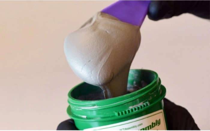
Solder paste is a mixture of flux and solder particles in a paste form. The viscosity of solder paste varies depending on the application. For example, higher viscosity paste is preferred when using a stencil. Other parameters of solder paste include solder particle size, cleaning type, lead-free properties, and melting point.
Placing the components on the circuit board involves positioning them on the pads. Before placing components, it’s essential to clean the stencil and PCB, typically with alcohol, to ensure that the stencil’s holes are not clogged and the PCB is free of contaminants. The next step is to mount the stencil on the printing station. The printing station can be purchased as a finished product, made in-house, or created using tools such as a 3D printer or laser cutter.
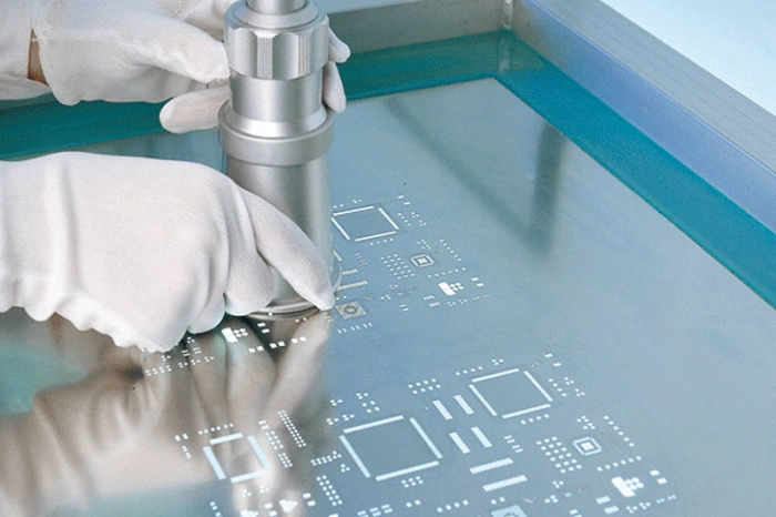
When applying solder paste, it’s crucial to align the stencil and PCB accurately and ensure the stencil is flat. Before applying solder paste, you can use cling film for a test run to avoid directly affecting the PCB. However, if you decide to apply solder paste directly, you must clean the PCB if unsatisfied with the result, as the paste can sometimes flow into the PCB’s vias, making it difficult to clean. The key to applying solder paste is to ensure there is enough paste. The squeegee should be large enough to cover the entire PCB, and the paste should be applied in a single smooth motion without repeated passes, which could cause the paste on the pads to smudge.
Component Placement
The simplest way to place components is with tweezers. If using an automated or semi-automated placement machine, the machine must be configured using data exported from the PCB CAD software. This includes generating a placement file for the machine and indexing the feeders. During placement, it’s important to ensure the components are correctly positioned, with the leads centered on the pads. Avoid pressing the components too hard into the paste, as it can squeeze out and cause defects like tombstoning or solder bridging. For BGA chip placement, check from all sides to avoid any visual misalignment. The usual sequence for placing components is to start with small components like resistors and capacitors, followed by larger components, with the largest through-hole components placed last.

Reflow Soldering
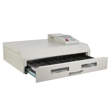
Reflow soldering is the next critical step, where the placed components are soldered by heating the solder paste to melt and bond the components to the PCB. This can be done using a pre-built heating station or a hot air blower. However, these tools have some issues, such as low heating efficiency and the risk of localized overheating. These problems are particularly pronounced in hot air blowers, where the PCB can be unevenly heated, possibly scorching the board. Also, these methods are unsuitable for double-sided PCB assembly. A more advanced reflow method uses a reflow oven, which can be purchased or custom-built, such as modifying a toaster oven. Commercial reflow ovens typically come in two types: infrared and hot air. Compared to heating plates and hot air blowers, ovens’ insulated chambers allow for more uniform preheating, bringing the entire board to the desired soldering temperature. Soldering follows a temperature profile often provided in the component’s datasheet. Typically, the profile includes a preheat phase, followed by a soak phase where the solder melts, then a quick cooling phase to solidify the solder. This temperature profile is especially important for temperature-sensitive components, preventing damage and ensuring stable electrical performance.
Another reflow method is vapor phase soldering, also known as condensation soldering. Unlike infrared or hot air, which can heat unevenly, vapor phase soldering uses a liquid medium called perfluoropolyether, a transparent oil. This liquid is heated to boil and generate steam, which heats the PCB to a stable temperature of 100°C at standard atmospheric pressure. Vapor phase soldering uses this steam to evenly heat the PCB, making it particularly friendly for soldering BGAs with hundreds or thousands of connections.
Double-Sided Component Placement
The simplest method for double-sided PCB assembly is to use glue to hold the components on the bottom side. The typical process involves mounting and soldering one side before doing the other. Another approach is to use solder with different melting points, where the solder on the bottom side has a higher melting point than the top. This way, during the second reflow, only the top-side solder melts, while the bottom remains intact. As previously mentioned, uneven heating with hot air or infrared methods can be used to achieve double-sided reflow soldering. By controlling the temperature on the top and bottom sides, even with the same solder, double-sided reflow can be accomplished. For small components like resistors, capacitors, and even smaller BGA or QFN packages, the surface tension of the molten solder will prevent them from falling off the bottom side.
Inspection
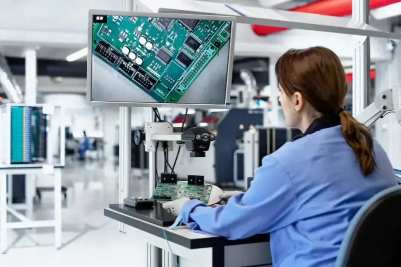
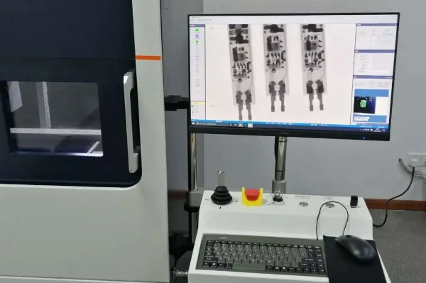
After soldering, the first step is not to power on the PCB, especially for boards with expensive components like FPGAs, which can cost thousands of dollars each. Instead, visual and optical inspections are performed first. Visual inspection checks for issues like solder bridging or tombstoning, while BGA solder joints require optical inspection, often using X-ray equipment, which is commonly used by Greatpcb.
PCB Manufacturability
Design for Manufacturing (DfM) can be considered from various angles. Firstly, components need sufficient spacing to avoid short circuits due to solder bridging after reflow. Secondly, avoid placing components near the PCB edges, as this can complicate solder paste application. Additionally, avoid unnecessary vias under BGA and QFN pads, as solder paste may flow into the vias and cause soldering issues. When placing test points, consider the reliability of the fixture, as misalignment could cause test failures. Also, avoid placing too many vias in thermal pads, as solder paste can escape into the vias, affecting solder quality. For PCBs with shielding covers, ensure that heat can be evenly distributed to solder the pads underneath successfully. Another important point is to minimize panelization, as different shrinkage rates may cause stress concentrations. Finally, pay attention to the design of the pads; they should not be too large or too small, as this could result in excessive or insufficient solder, affecting the soldering quality.
Table of Contents
Related Posts
PCBA Prototype
January 25, 2026
PCBA Prototype
December 8, 2025


