Do You Understand the Various Symbols on PCB Boards?

Symbols on PCB boards are divided into component symbols, electrical connection symbols, labeling and indication symbols, and special function symbols. These symbols carry crucial information for design, production, assembly, and troubleshooting, and are essential for the reliable operation of electronic products.
Introduction
In the “heart” of electronic devices — the PCB (Printed Circuit Board), you’ll find a variety of symbols. While these symbols might seem mysterious at first glance, they are, in fact, the key language through which engineers “communicate” with the circuit board. They carry vital information that plays a significant role in PCB design, production, assembly, and troubleshooting.
1. Common Symbol Categories
Symbols on PCB boards can be broadly categorized into:
- Component symbols
- Electrical connection symbols
- Labeling and indication symbols
- Special function symbols
This classification helps us systematically organize their meanings and clarify their roles in the circuit’s operation.
2. Types of Symbols and Their Meanings
Component Symbols:
- Resistor Symbol (R): Represented by a rectangle or a zigzag line, the resistor is one of the most common component symbols on a PCB. It is used to limit current, divide voltage, and other functions. Resistors with different resistance values are labeled with numbers such as “R1,” “R2,” etc., for easy identification during circuit design and maintenance. In a simple LED current-limiting circuit, the resistor controls the current flowing to the LED, ensuring it works properly and isn’t damaged.
- Capacitor Symbol (C): Often represented by two parallel lines or a circle, capacitors are used for storing charge, filtering, and coupling. Electrolytic capacitors have positive and negative terminals, which are clearly marked with “+” and “-“, while small ceramic capacitors are often used in high-frequency signal processing to maintain signal purity.
- Inductor Symbol (L): Typically shown as a coil, inductors work based on electromagnetic induction. They store energy, filter signals, and match impedance in circuits. In RF circuits, inductors work with capacitors to form resonant circuits that filter signals within a specific frequency range, aiding efficient wireless communication.
- Integrated Circuit (IC) Symbol: IC symbols are more complex, often rectangular or square, with internal details varying according to the chip’s function. ICs integrate numerous transistors and other components to perform complex logic operations and signal processing. For instance, processors on mobile phone motherboards act as the core “brain” of the device, handling data computation and command execution.
Electrical Connection Symbols:
- Wire Symbol: Represented by a straight line, wires connect the pins of various components and serve as the “pathways” for current and signal transmission. In multi-layer PCBs, vias (represented by circular or oval symbols) are used to connect the circuits on different layers, ensuring smooth routing.
- Power and Ground Symbols: The power supply is typically marked as “VCC” or “VDD,” indicating the positive supply, while the ground symbol resembles an inverted triangle or three short horizontal lines. Ground provides a reference zero voltage and serves as the return path for signals and charge discharge, maintaining overall circuit stability.
Labeling and Indication Symbols:
- Component Position Labeling: Symbols like “R1” and “C2” help engineers quickly locate components during assembly or repair by referring to the PCB layout diagram, enhancing efficiency.
- Test Point Symbol: Often represented by a solid circle or square with the label “TP,” test points are used for signal measurement and troubleshooting with tools like oscilloscopes and multimeters.
Special Function Symbols:
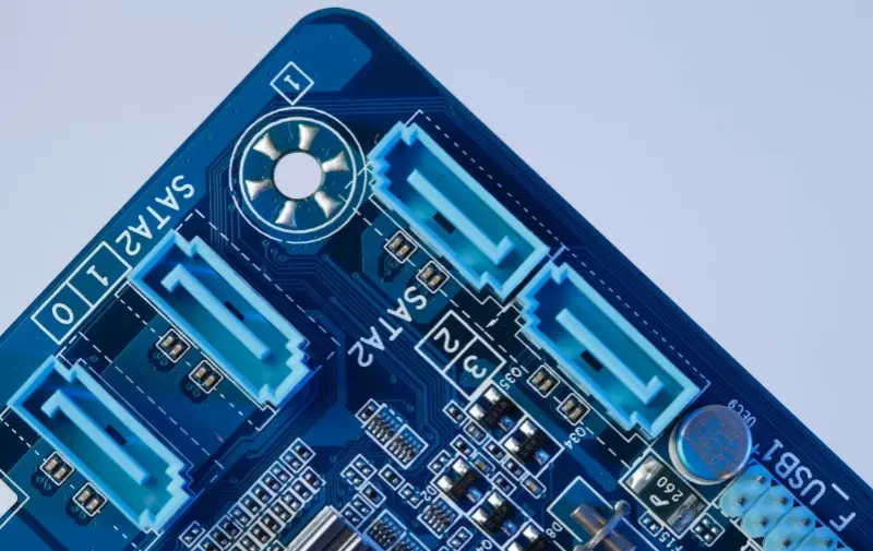
- Silkscreen Marks: These include text and patterns that display component models, polarity indications, company logos, and more. They assist with accurate component placement during production, as well as help with product traceability and brand display.
- Solder Mask Symbols: Areas on the PCB where solder paste is not applied are marked with specific shapes (such as outline boxes), indicating that the surface will not be covered with solder to protect traces and avoid shorts, ensuring precise and controlled soldering during production.
Conclusion
The symbols on a PCB act as a detailed map and operation guide — from outlining the electrical blueprint during circuit design, to guiding component soldering and placement during production, and finally, aiding troubleshooting during after-sales maintenance. Understanding these symbols allows electronic professionals to navigate the “circuit board world” skillfully and ensures the reliable performance of electronic products.
Related Posts
PCBA Prototype
December 8, 2025
PCBA Prototype
November 9, 2025


