Low Temperature Co-fired Ceramic (LTCC) Substrate Circuit Processing Technology

1. Overview of LTCC Substrate Circuits
Low Temperature Co-fired Ceramic (LTCC) technology, first introduced in the mid-1980s in the United States, is a multi-layer ceramic manufacturing technology that integrates interconnection, passive components, and packaging into one. With continuous advances in science and technology, electronic products are becoming smaller, thinner, and more powerful. For example, in the wireless communication industry of mobile phones, the size of the phones has reduced significantly. Early mobile phones were used for basic audio transmission, while today they have evolved into handheld network computers. By integrating some passive components into the substrate, not only can system miniaturization be achieved, but it also increases circuit assembly density and system reliability.
Currently, integrated packaging technologies include thin-film technology, silicon semiconductor technology, multi-layer circuit board technology, and LTCC technology. LTCC technology provides a low-cost packaging solution with a short development cycle. LTCC technology meets the needs of lightweight, thin, short, and small products. However, LTCC substrates have high hardness and brittleness. When cutting these hard substrates, significant friction occurs between the cutting machine and the substrate, transferring stress onto the cutting blade. This results in a decrease in product yield and qualification rate for LTCC-based electronic products. Therefore, improving the yield of products when ceramic substrates are cut is an important issue.
2. LTCC Substrate Manufacturing Process
Figure 2 shows the process flow for manufacturing LTCC substrates, which includes major steps such as mixing, casting, drilling, hole filling, screen printing, lamination, isostatic pressing, and sintering. Below is a brief introduction to each process.
Mixing and Casting: Organic materials (mainly polymer binders and plasticizers dissolved in a solution) and inorganic materials (ceramics and glass) are mixed in specific proportions. The mixture is ball-milled for uniformity, then poured onto a moving carrier film (typically polyester) and passed through a drying zone to remove solvents. The desired thickness is achieved by controlling the doctor blade gap. The typical thickness tolerance of this process is ±6%.
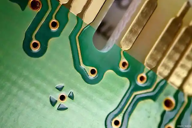
Drilling: Mechanical punching, drilling, or laser drilling is used to create vias. Vias are small holes (typically 0.1-0.2mm in diameter) drilled into green ceramic sheets to interconnect circuits on different layers. Molds are also created at this stage to assist alignment during lamination and to automatically align the conductor and dielectric during printing.
Printing: Standard thick-film printing technology is used to print conductor paste and then dry it. Vias and conductor patterns are dried in a box or chain furnace at the appropriate temperature and time. All resistors, capacitors, and inductors are also printed and dried at this stage.
Via Filling: Traditional thick-film screen printing or stencil extrusion is used to fill vias with a specially formulated conductor paste that has a high solid content.
Degassing and Sintering: The organic binders are removed in the 200-500°C range, referred to as the organic removal zone (it is recommended to maintain the stack at least 60 minutes in this zone). After this, the stack is co-fired at the peak temperature (typically 850°C) for 5-15 minutes. The sintering process typically takes 2-10 hours, depending on the metalization and degassing curve. After sintering, the components are ready for further processing, such as printing conductors and precision resistors on the top surface and firing them in air. If copper is used for metallization, the sintering must be done in a nitrogen chain furnace.
Inspection: The circuit is then laser adjusted (if necessary), tested, sliced, and inspected. In LTCC packaging, hard soldered leads or heat sinks may be used (if required).
3. LTCC Substrate Circuit Processing Cases
3.1 Micro Via Formation Technology for LTCC Substrates
The formation of micro vias is a key process in the high-density interconnection of multi-layer LTCC substrates, as the size and position accuracy of the vias directly impact the wiring density and substrate quality. To achieve ultra-high density, the via diameter should be smaller than 100μm. Methods for creating micro vias in LTCC green tapes include mechanical punching and laser drilling.
3.1.1 Mechanical Punching
CNC punching is an effective method for forming vias in green ceramic tapes, particularly for standardized products, where punching is more advantageous. A punching die can create thousands of holes at once, with a minimum hole diameter of 50μm. Punching speed is fast, and the precision is relatively high, making it suitable for mass production. During the creation of micro vias, a punch and die with matching sizes are used. The opening of the die is typically 12.5μm larger than the diameter of the punch.
The key technical points for making micro vias include properly installing and operating the small punch. When the punch diameter is less than 100μm, the punch becomes fragile and difficult to handle. Most punching defects are caused by improper handling rather than the punching process itself. Therefore, special tools are required to install and operate the small punch and to prevent damage during handling. The alignment between the punch and die is crucial for producing high-quality vias. If misaligned, the via quality will suffer, and both the die and punch may be damaged.
The quality of mechanical punching-created micro vias is consistent in terms of hole size and spacing. The top edge is smooth, while the bottom edge is rougher, and the internal wall is straight. The size consistency holds for different thicknesses of LTCC green tapes. For example, micro vias with diameters of 50, 75, and 100μm formed in LTCC tapes of thicknesses ranging from 50 to 254μm exhibit consistent results.
3.1.2 Laser Drilling
Laser drilling works by focusing laser beams along the edges of the vias, emitting continuous light pulses that vaporize the ceramic material layer by layer until a via is formed. This method is ideal for drilling LTCC green tapes. CO2 lasers are commonly used, as their high power easily vaporizes the organic binder in the green tape, with minimal impact on the tape itself. The minimum hole diameter achievable is 50μm.
Laser drilling creates conical vias, with the via diameter on the back side of the tape decreasing as the tape thickness increases, due to the limited precision of the laser beam. For thicker LTCC tapes, it becomes more difficult to create small vias with acceptable precision. To form smaller vias on thicker tapes, the laser beam must be finely adjusted to make the inner wall of the via straighter, avoiding a conical shape. Laser-drilled vias smaller than 50μm have poor via-through connectivity, and 75μm vias may have residual material that affects the quality of the via.
3.2 LTCC Substrate Micro Via Filling Methods
3.2.1 Mask Printing Method
The mask printing method is suitable for high-density wiring LTCC substrates. The mask material is typically made of 0.03-0.05mm thick brass, stainless steel, or polyester film, with vias etched into it. The via paste is loaded into a bladder, and the mask is positioned on the ceramic tape. The paste is then pressed through the mask by applying air pressure to the bladder, filling the vias. This method achieves a high-quality fill, especially for vias larger than 100μm.
For vias smaller than 100μm, multiple printings and adjustments in pressure and other settings are required. Additionally, adjusting the mask opening to suit the via size is necessary for optimal filling. For example, larger mask openings are used for 100μm vias to maximize vertical filling.
3.2.2 Micro Via Injection Method
The micro via injection method generally offers the best results but requires specialized equipment. Factors affecting the quality of via filling include injection pressure, injection time, paste viscosity, and alignment between the LTCC tape and the filling mask. Once the parameters are set, thousands of vias can be filled within seconds.
Defects such as unfilled, overfilled, and underfilled vias must be monitored. Unfilled vias can be identified by backlighting, and overfilled vias are those with paste extending beyond the via boundary. If vias are overfilled between neighboring holes, the via spacing must be increased to prevent short-circuiting. However, this may reduce internal interconnection density.
3.3 LTCC Substrate Degassing and Sintering
The key to successful sintering is controlling the shrinkage rate and the overall change of the substrate during sintering. LTCC sintering typically uses methods such as controlling powder particle size, binder proportion, heat press lamination pressure, and sintering curve. However, LTCC substrates still shrink along the X-Y axis by 12-16%, even with these methods. Zero-shrinkage materials can be achieved using technologies like pressure-assisted sintering or sintering without pressure.
Various processes, such as self-restraining sintering, pressure-assisted sintering, and composite sintering, have been developed to control shrinkage and meet the needs of different performance products.
3.4 LTCC Substrate Large Area Ground Soldering
The design of the large area ground soldering process for LTCC substrates involves improving the solderability and reliability by applying a composite metal film (Ni+M) on the ground plane. Compared with conventional metallized ground layers, the solderability is significantly improved (>600s). This method is critical for improving the quality and longevity of the LTCC packaging.
Table of Contents
Related Posts
PCBA Prototype
April 6, 2025


