PCB etching process and chemical reaction formula
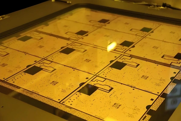
As the PCB industry develops, the demand for precise control over trace impedance has increased, necessitating stricter control over trace width. PCBs are becoming more reliable and widely used in everyday life, with designs becoming increasingly diverse and sophisticated. Etching technology is also becoming more prevalent in PCB design. This technique utilizes the photosensitivity of chemical materials, where a photosensitive layer is applied evenly to both sides of the metal substrate. The pattern is then precisely transferred onto the photosensitive layer using photolithography, and the unexposed areas are developed and removed. The exposed metal areas are then etched away by direct contact with an etchant, resulting in the desired geometric shapes and high-precision dimensions.
What is PCB Etching?
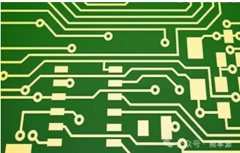
Etching is one of the most crucial processes in PCB manufacturing. Simply put, wet PCB etching is a controlled corrosion process. Under normal circumstances, corrosion damages metal, but with an effective processing technique, it can be controlled, and this process is called etching. PCB etching involves removing unwanted copper (Cu) from the circuit board. Unwanted copper refers to the non-circuit copper that is removed from the board according to the PCB design, resulting in the desired circuit pattern.
In other words, etching is like carving a circuit board. Imagine the board as a rock, and etching is the process of chiseling the rock into a beautiful sculpture. During this process, the base copper or starting copper is removed from the board. Rolled and annealed copper is easier to etch away than electroplated copper.
Before the etching process begins, the layout is prepared. There are two different methods for inner and outer layer etching. In the outer layer etching process, the plated layer serves as the resist, while in the inner layer, a photoresist acts as the resist.
Process Flow
The PCB etching process typically involves the following steps: photoresist application, development, etching, resist stripping, and cleaning.
- Photoresist Application: A layer of photoresist is applied to the copper layer to protect the areas that should not be etched. The photoresist can be applied using photolithography or screen printing techniques.
- Development: The photoresist-covered copper layer is developed, removing the unwanted portions of the photoresist and leaving only the areas that need to be etched.
- Etching: The PCB is then placed in an etching tank, where the etchant removes the unwanted copper, forming the desired circuit pattern.
- Resist Stripping: After etching, the remaining photoresist is removed from the PCB, typically using chemical solvents or thermal desorption.
- Cleaning: Finally, the PCB is cleaned to remove any remaining etchant and other contaminants, ensuring a clean surface.

Overview of PCB Etching Processes
Alkaline Etching Process:
The alkaline method is used for etching the outer layers of a PCB. The chemicals involved include copper chloride (CuCl2), hydrochloric acid (HCl), hydrogen peroxide (H2O2), and water (H2O). The alkaline method is a fast process but also somewhat expensive. The process parameters must be carefully controlled, as prolonged exposure to the solvent can damage the circuit board.
- Main Components: Copper chloride, ammonia, ammonium chloride, a small amount of oxidizer, and inhibitors.
- Applicable Fields: Typically used for creating outer layer circuit patterns in multilayer PCBs or for direct etching of microwave PCB patterns using a negative film method.
- Key Features:
- The etching rate is easily controlled, achieving high etching quality under stable conditions.
- High copper dissolution capacity.
- The etchant is easily regenerated and recycled, reducing pollution. Key control points include temperature, specific gravity, and pH value.
- Etching Rate: Approximately 1 mil/min.
- Main Reaction Mechanism:Copper Etching Reaction: Copper can exist in three oxidation states: metallic Cu on the board surface, blue copper ions Cu(NH₃)₄²⁺ in the etching tank solution, and the intermediate cuprous ions Cu(NH₃)₂⁺. Metallic copper Cu can be oxidized and dissolved in the etching tank solution by Cu(NH₃)₄²⁺, completing the copper etching reaction, as shown in the following reaction:2Cu+2Cu(NH3)4Cl2→4Cu(NH3)2Cl (cuprous ion)2Cu + 2Cu(NH₃)₄Cl_2 \rightarrow 4Cu(NH₃)₂Cl \, (\text{cuprous ion})2Cu+2Cu(NH3)4Cl2→4Cu(NH3)2Cl(cuprous ion)Regeneration Reaction: The intermediate cuprous ion Cu(NH₃)₂⁺ formed in the above reaction is a light blue, muddy precipitate with poor solubility. If not removed quickly, it can create a barrier to copper etching on the board surface. To avoid this, additional etching solution (ammonium chloride and ammonia) and a large amount of oxygen from the air are used to oxidize it into soluble Cu(NH₃)₄²⁺, which continues to act as an oxidizer in the copper etching reaction. This is the recycling and regeneration reaction of the etchant, as shown below:4Cu(NH3)2Cl+4NH3+4NH4Cl+O2→4Cu(NH3)4Cl2+2H2O4Cu(NH₃)₂Cl + 4NH₃ + 4NH₄Cl + O₂ \rightarrow 4Cu(NH₃)₄Cl_2 + 2H₂O4Cu(NH3)2Cl+4NH3+4NH4Cl+O2→4Cu(NH3)4Cl2+2H2ONet Reaction:2Cu+4NH3+4NH4Cl+O2→4Cu(NH3)4Cl2+2H2O2Cu + 4NH₃ + 4NH₄Cl + O₂ \rightarrow 4Cu(NH₃)₄Cl_2 + 2H₂O2Cu+4NH3+4NH4Cl+O2→4Cu(NH3)4Cl2+2H2OEtching Process: The entire process is carried out in a conveyor-type high-pressure spray etching chamber, where the PCB is exposed to fresh etchant spray. In the alkaline PCB etching process, certain key parameters need to be considered, such as the rate of panel movement, chemical spray, and the amount of copper to be etched away. This ensures that the etching process uniformly completes the sidewalls.The point where the unwanted copper is fully etched away is known as the breakpoint. This typically occurs at the midpoint of the etching chamber. For example, if the etching chamber is 2 meters long, the breakpoint would be reached when the board reaches the midpoint, i.e., 1 meter.
Acidic Etching:
The acidic method is used for etching the inner layers of rigid PCBs. This method involves chemical solvents such as ferric chloride (FeCl₃) or copper chloride (CuCl₂). Compared to the alkaline method, the acidic method is more precise and cheaper but more time-consuming. This method is suitable for inner layers because the acid does not react with the photoresist and does not damage the desired areas. Additionally, undercutting is minimal in this method. Undercutting is the lateral erosion of the etching material beneath the resist layer. When the solution contacts copper, it attacks the copper and leaves the protected tracks. The tracks are protected by either electroplated resist or photo-imageable resist. At the edges of the tracks, a certain amount of copper beneath the resist is always removed, which is known as undercutting.
- Main Components: Copper chloride, hydrochloric acid, sodium chloride, or ammonium chloride.
- Applicable Fields: Typically used for creating inner layer circuit patterns in multilayer PCBs and etching pure tin PCBs, or in the full-plate electroplating + dry film negative production process.
- Key Features:
- Widely used system with mature processes in terms of capacity, recycling control, and usage methods. However, since the regeneration rate of ferrous chloride into ferric chloride is slower, the production speed is only half that of ammoniacal copper. It also corrodes etching resists such as lead-tin and pure tin, making it more suitable for inner layers and single-sided PCB etching. The process also generates chlorine gas, leading some PCB manufacturers to adopt the negative film + acid etching process to meet deadlines and efficiency goals.
- Etching Rate: 0.5 mil/min.
- Main Reaction Mechanism:Copper Etching Reaction: Copper can exist in three oxidation states: metallic copper Cu⁰ on the board surface, blue copper ions Cu²⁺ in the etching tank solution, and the less common cuprous ions Cu⁺. Metallic copper Cu⁰ can be oxidized and dissolved in the etching tank solution by Cu²⁺, as shown in the following reaction:3Cu+3CuCl2→6CuCl3Cu + 3CuCl_2 \rightarrow 6CuCl3Cu+3CuCl2→6CuClRegeneration Reaction: The Cu⁺ formed in the etching reaction is further oxidized by the oxidizer and HCl in the etching tank, converting back into Cu²⁺, which continues to react with the metallic copper on the board surface. This regeneration ensures that the etching solution can etch away more metallic copper Cu⁰. This recycling and regeneration reaction is shown below:6CuCl+NaClO3+6HCl→6CuCl2+3H2O+NaCl6CuCl + NaClO_3 + 6HCl \rightarrow 6CuCl_2 + 3H₂O + NaCl6CuCl+NaClO3+6HCl→6CuCl2+3H2O+NaClNet Reaction:3Cu+NaClO3+6HCl→3CuCl2+3H2O+NaCl3Cu + NaClO_3 + 6HCl \rightarrow 3CuCl_2 + 3H₂O + NaCl3Cu+NaClO3+6HCl→3CuCl2+3H2O+NaCl
Ferric Chloride Etching
Due to the high treatment costs associated with copper etchants, the use of ferric chloride etchant is limited in industrial applications. However, ferric chloride is an attractive spray etchant because of its ease of use, copper retention capability, and suitability for infrequent batch applications. Ferric chloride can be used with screen inks, photoresists, and gold patterns but is incompatible with tin or tin/lead resists.
Ferric chloride solution is typically dissolved in water at a concentration range of 28-42% (by weight). HCl (up to 5%) is also mixed with the solution to prevent the formation of insoluble ferric hydroxide precipitates.
The commonly used ferric chloride has a specific gravity of 36 Be or approximately 4.0 lb/gal FeCl3. Commercial acid (HCl) content is typically within the range of 1.5-2%.
Main Components
Ferric Chloride, Hydrochloric Acid
Application Areas
Generally used for single-sided PCB production
Main Characteristics
Due to the need for chlorine gas in recycling, low unit volume capacity, difficult control, and slow etching speed, it is mostly used in single-sided PCB manufacturing.
Control Focus
Specific Gravity and pH Value
Primary Reaction Mechanism
Etching Mechanism:
FeCl₃ + Cu → FeCl₂ + CuCl
FeCl₃ + CuCl → FeCl₂ + CuCl₂
CuCl₂ + Cu → 2 CuCl
Factors Affecting Etching Rate
- Influence of Fe³⁺ Concentration: The concentration of Fe³⁺ has a significant impact on the etching rate. As the concentration of Fe³⁺ in the etching solution increases, the etching rate of copper increases accordingly. However, when the concentration exceeds a certain level, the increased viscosity of the solution may reduce the etching rate.
- Influence of Etching Solution Temperature: The higher the temperature of the etching solution, the faster the etching rate. The temperature should be selected to avoid damaging the resist layer, generally within the range of 40-50°C.
- Influence of Hydrochloric Acid Addition: Adding hydrochloric acid to the etching solution can inhibit the hydrolysis of FeCl₃ and increase the etching rate. This effect is particularly noticeable when the dissolved copper concentration reaches 37.4g/L. However, the amount of hydrochloric acid added must be appropriate, as excessive acidity can damage the liquid photoresist coating.
- Etching Solution Agitation: The efficiency and quality of static etching are poor because precipitates form on the surface and in the solution during etching, causing the solution to turn dark green. These precipitates can interfere with further etching.
Ammonium/Sodium Persulfate Micro-Etching
Main Components
Ammonium Persulfate, Sulfuric Acid / Sodium Persulfate, Sulfuric Acid
Application Areas
Generally used for micro-etching of inner and outer layer circuit patterns in multilayer PCBs.
Primary Reaction Mechanism
Na₂S₂O₈ + Cu → CuSO₄ + Na₂SO₄
Main Characteristics and Considerations
The sodium persulfate micro-etching system has replaced the ammonium persulfate system for over 20 years, as sodium persulfate does not form ammonium-copper complexes that complicate wastewater treatment and creates a more uniform roughened surface. It is typically set at approximately 100±10g/L sodium persulfate, 1-3% sulfuric acid, and 35°C±2°C, with an etching time of 60-120 seconds, micro-etch depth of 0.375-2µm, copper control limit <20g/L, and an etching rate of approximately 0.5-2µm/mil. However, it cannot be recovered using copper sulfate recovery systems; if the copper concentration exceeds the set value, the tank must be replaced.
The etching rate of sodium persulfate increases when the copper concentration exceeds 0.75g/L, with the rate rising from 0.2µm/mil to 0.25µm/mil. As a result, controlling the etching rate of sodium persulfate is challenging. To address this variability, some manufacturers have developed stabilized persulfate systems by adding 5-15g/L stabilizers to the solution.
Hydrogen Peroxide Micro-Etching
Hydrogen peroxide micro-etching is recyclable, ammonia-free, and has lower costs. The sulfuric acid + hydrogen peroxide micro-etching system has a copper load capacity of approximately 50g/L, reducing environmental impact. However, the tendency of hydrogen peroxide to decompose during use limits its widespread application. To counteract this, stabilizers are added to the solution to prevent hydrogen peroxide decomposition, ensuring a consistent micro-etching rate.
Main Components
Hydrogen Peroxide, Sulfuric Acid
Application Areas
Generally used for micro-etching of inner and outer layer circuit patterns in multilayer PCBs.
Main Function
Cleaning the board surface and roughening the copper surface
Primary Reaction Mechanism
Cu + H₂O₂ → CuO + H₂O
CuO + H₂SO₄ → CuSO₄ + H₂O
Main Characteristics and Considerations
Hydrogen peroxide is an oxidizing solution, but its instability necessitates the addition of stabilizers and promoters. The copper ions generated during etching are surrounded by sulfate ions, facilitating crystal formation and copper recovery. This etching process generally occurs at 40°C; lower temperatures slow the reaction, while higher temperatures affect the etching factors. Hydrogen peroxide concentration is set at 5-10%, and sulfuric acid concentration at 10%. The copper concentration in the etching solution rises as etching progresses, typically limited to below 50g/L. As copper concentration increases, hydrogen peroxide concentration decreases, making copper ion control a critical parameter in micro-etching solutions.
The drawbacks of hydrogen peroxide include poor stabilizer performance, which may cause epoxy bonds to break at high temperatures, and the catalytic effect of divalent copper producing water molecules and oxygen. To prevent hydrogen peroxide decomposition, stabilizers must be added to the solution. The instability of hydrogen peroxide arises from the production of free radicals, which accelerate chain reactions. Stabilizers help neutralize free radicals, inhibiting decomposition reactions.
PCB Etching Factors and Testing Frequency
Before performing PCB etching, it is necessary to determine the etching factor and testing frequency.
Etching Factor
The etching factor refers to the amount of substrate consumed by the etchant during the etching process. The size of the etching factor has a significant impact on the etching result, requiring testing and control. Generally, the etching factor ranges between 0.1 and 0.3. If the etching factor is too large, the etching process may become too aggressive, potentially damaging the PCB. If the etching factor is too small, the coating may not be fully removed, affecting the quality of the circuit board.
Testing Frequency
Testing frequency refers to how often data sampling and testing are conducted during the etching process. The choice of testing frequency should be adjusted based on specific conditions. For general PCB manufacturing, a testing frequency of 100-1000Hz can be selected. A frequency that is too low may result in inaccurate data sampling, making it difficult to monitor the etching process. Conversely, a frequency that is too high may increase production costs, but for high-precision PCB manufacturing, the testing frequency can be appropriately increased to ensure the accuracy of etching results.


