Why Signal Traces Should Not Cross Plane Splits?

One crucial rule in PCB design that cannot be emphasized enough is: Never route signals across split planes. This principle has been stressed in many PCB design tutorials, but unfortunately, it’s still common to see designers violate this rule.
In PCB design, sometimes splitting planes is unavoidable. For example, to separate digital circuits from analog circuits, it’s common to split the ground plane. In multi-layer PCBs, there are often multiple power planes, so it is even more common to split the power planes. In these cases, if signal traces cross the split ground or power plane, you need to be cautious.
Especially when signal traces are referenced to a power plane, it’s inevitable that they will cross the split. The circuit might still work, but it will not work well. You might not have considered issues like EMC (electromagnetic compatibility), radiation, or noise interference. Once those problems appear, diagnosing them can be very challenging. In low-frequency circuits, the effect might be minimal, but routing signals across split planes is not a good habit.
In high-speed circuit design, this rule should definitely be avoided. The reason why people forget about this rule is not because the theory is unclear, but because the explanation doesn’t leave a lasting impression, and people don’t take it seriously enough. Today, let’s use ADS (Advanced Design System) to demonstrate.
Step-by-step explanation with ADS simulation:
- Create a 4-layer PCB stackup: The top and bottom layers are signal layers, and the inner two layers are ground and power planes.
- Lay out a microstrip line: Since this is a simple simulation, we don’t need to focus too much on characteristic impedance. The signal trace on the top layer is roughly defined.
- Add a large copper pour as the ground plane: In the second layer, cut a narrow slit in the ground plane to simulate a split.

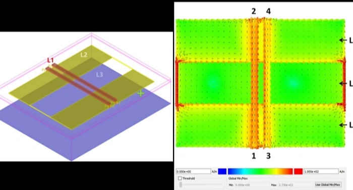
After running the simulation, you can observe the current distribution of the return current on the ground plane. The signal current on the top layer flows from right to left, and the return current on the second layer flows from left to right. When the return current crosses the split gap, it flows along the edges of the gap, as this provides the lowest impedance path for the current.

Wherever current flows, a magnetic field will be generated. The following simulation shows the magnetic field distribution, where the return current, as it crosses the split gap, deviates from the signal trace. You can imagine that the electromagnetic wave energy is no longer controlled by the signal trace and the ground plane, but leaks out.

By carefully analyzing the simulation, you’ll also notice that the level of this noise is influenced by the size of the gap, the distance between the PCB layers (L1, L2, L3, etc.), and the distance between the signal line and the reference plane. If you select thinner dielectrics and keep the distance between the signal line and the reference plane small, and control the gap to below 5 mils, it will greatly reduce the impact of routing across the split plane. However, this approach will increase the cost. Despite this, some return current will still flow along the gap edges and cause electromagnetic interference. Therefore, it’s crucial to avoid routing signals across split planes.

Example of Differential Transmission Line:
Let’s take a look at this 2D diagram, which shows the current distribution when two differential transmission lines (balanced transmission lines) cross a split area. The signal traces are on L1 and L2, which are ground planes, and there is a cut in the middle. L3 is the reference plane of the next layer. When one of the differential transmission lines is driven and the other one is terminated, the return current on either side of the split between L2 and L3 flows in opposite directions, causing crosstalk.

#image_title
When the differential transmission line is driven in a differential mode, the current direction in both lines is opposite, and the return current flows along the gap in the split plane. The current direction in L2 is the same on both sides of the split, while the current on L3 flows in the same direction. By analyzing this, you can observe that the differential signal has generated common-mode noise. This noise not only radiates into free space, causing EMI (electromagnetic interference), but it also disturbs the differential signal, causing a phenomenon called “skew.”
Differential signal integrity is compromised because the differential transmission line on the PCB behaves differently from the tightly coupled twisted pair of wires. The coupling between the differential signal lines can be loose or tight, but the differential signal’s integrity heavily depends on the integrity of the reference plane.
Related Posts
PCBA Prototype
December 14, 2025
PCB Assembly
September 2, 2025


