PCB Trace Width Calculator: How to Use?

Do you know that you need to set the PCB trace width calculator to avoid damage? Are you aware that the trace width determines the amount of current you can carry? As a PCB enthusiast, you should be mindful of these factors to succeed in your PCB manufacturing projects.
If you don’t follow the appropriate rules for setting, you may end up designing ineffective or faulty PCBs. We created this article to help you use the PCB trace width calculator to find the trace width for your PCB. Additionally, this article covers formulas and common questions to help you determine the width yourself.
1. What is a PCB Trace Width Calculator?
A PCB trace width calculator is a tool that determines the PCB trace width based on the CIP 2221 formula. Trace width is a key factor to consider when designing printed circuit boards. In fact, you must assign the correct width to the traces to prevent them from being damaged by high temperatures.
It’s best to design traces on the PCB to handle maximum current loads before any failures occur. Keep in mind that when you conduct more current through a path, it begins to heat up. Therefore, when the current load exceeds the limit, the trace can burn out or damage the PCB laminate, which may lead to permanent PCB damage.
You can compare PCB traces to wires connecting various zero-resistance components. However, each PCB path has its own resistance, which is an essential factor in choosing the PCB trace width. Thus, you need to understand resistance and current capacity to define the width you will use.
It’s important to note that temperature increases can affect trace width. Temperature rise refers to the temperature of the trace when current is on versus when it’s off. In other words, simply subtract the working temperature from a higher working temperature to obtain the temperature rise.
We understand that finding the trace width may seem like a daunting task, right? However, you need not worry! The trace width calculator simplifies the entire process quickly and accurately.
2. How to Calculate PCB Trace Width
It’s not enough to simply find the available trace on the circuit board or use simple methods to accurately identify its trace resistance. To ensure the trace on the circuit board opens correctly, you need to determine the width of your PCB traces. Setting and significantly increasing the PCB trace width will minimize the resistance of the circuit board traces.
2.1 What You Need to Know Before Using the PCB Trace Width Calculator
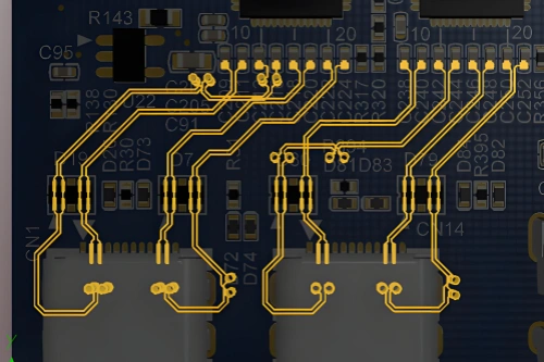
Determining the width of the PCB traces is much more complex than finding a specific conductor. This is because many factors need to be considered before calculating the trace width on the circuit board. For example, you should know the maximum current that the PCB can operate with, such as the thickness of the trace.
2.2 Width and Spacing of PCB Traces
To use the PCB trace width calculator to get the trace width, you need to consider the following factors:
- Current carrying capacity of the trace.
- The spacing and size of the pads to which your trace will connect.
- The space between traces. In addition to the trace width, it is equally important to check the space between traces to prevent short circuits and leave maximum space between traces for effective conduction.
In terms of production cost, circuit boards are typically small. However, if your PCB is too small, you will face challenges in routing the traces and maintaining proper spacing between them. Most PCB manufacturers recommend a gap of 6 to 30 mils for many trace widths.
2.3 Trace Width Formula for PCB Calculator
You can still use the trace width formula to determine the trace width of the PCB. This method allows you to calculate the permissible current that can be carried by a specific trace. The CIF 2221 standard defines the formula as follows:
I = k × (ΔT)0.44 × (A)0.725
Where:
- I represents “current,” which you should always consider as a constant.
- ΔT represents the change in temperature, while A represents the cross-sectional area of the trace.
It’s important to note that you can rearrange the equation to establish the width of the trace by determining the specific cross-sectional area that allows for safe current flow.
Area (mils2) =
(Current (Amps) / (k × (Temperature Rise (°C))0.44))0.725
Width (mils) = Area (mils2) / (Thickness (oz) × 1.378 (mils/oz))
You can use the PCB trace width formula for 0-35 Amps as it allows a temperature rise from 100°C to 1000°C. Additionally, the formula also considers a trace width of 400 mils.
Disclaimer: Most PCB manufacturers use the PCB trace width formula as an industry standard and consider it correct. However, it may not suit all designs. Therefore, please note that we are not liable for any losses you incur.
3. Common Questions About Trace Width Calculators
Q: Does the PCB trace calculator have limitations on current?
A: The CIF 2221 standard derived by engineers accommodates currents up to 35 Amps, with a maximum trace width of 400 mils and a moderate rise of 10-1000°C, with copper content of 0.5-3 Oz/m².
Q: What does temperature rise mean in this context?
A: The temperature rise here refers to the difference between the optimal operating temperature of the PCB and the standard operating temperature. It’s essential to recognize that increased current transmission will raise the trace temperature. Thus, temperature rise is a design factor that guides you in enhancing the thermal capacity of the PCB.
Q: What is a mil?
A: Essentially, you can define a mil as 1/1000 of an inch, which is a standard measurement term in the electronics world.
Conclusion
Printed circuit boards form the backbone of various electronic products. We hope you now realize the need to set the trace width for your PCBs to prevent damage. Setting the trace width will also enable you to determine the current capacity of the traces. Remember, you must adhere to all the established standards discussed above to create a good PCB.
Related Posts
PCBA Prototype
December 14, 2025
PCB Assembly
September 2, 2025


