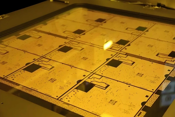
High-Speed USB Design on a Two-Layer PCB
In our previous article, "Experience Formulas in PCB Design" we introduced some practical formulas. Now, let’s dive into a real-world application by focusing on high-speed USB design on a [...]
Can Signal Attenuation Occur Even in PCB Traces with Near-Zero Resistance? When designing high-speed PCBs, signal integrity is a key concern. Signal integrity refers to the ability of a [...]
3W Rule To reduce crosstalk between traces, the spacing between them should be sufficiently large. When the center-to-center distance between traces is at least three times the trace width, approximately [...]
When you learn to design high-speed PCBs, it signifies that you can move beyond simple single-chip circuits and tackle more complex embedded systems. While learning high-speed PCB design involves numerous [...]
In circuit design, it's common to see resistors in series with the data lines (D+ and D−) of USB interfaces on schematics. These resistors are often explained as being for [...]
The PCB half hole is widely used in the PCB manufacture of modern circuit boards, which can make the connection between electronic circuit board components close, and also enhance the [...]
In PCB design rules, there are numerous empirical formulas for designers to reference. However, is there a simpler method to address practical issues? Even if a ground copper plane has [...]
It is widely known that PCB routing should avoid right angles or acute angles. This rule is emphasized in textbooks and company technical specifications, and some even use it as [...]