Understanding Dead Copper on PCBs: Causes, Effects, and Solutions

What is Dead Copper on a PCB?
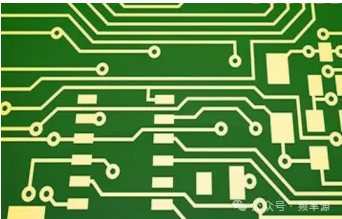
Dead copper refers to areas on a copper layer of a printed circuit board (PCB) that are unable to conduct electrical current. These areas often do not align with the intended circuit paths, resulting in impeded or blocked current flow. Dead copper may occur due to incomplete coverage of the copper layer, manufacturing process errors, or design flaws. Dead copper is also known as PCB islands, which are isolated copper foils within the PCB, typically formed during copper pouring.
Causes of Dead Copper
- Manufacturing Process Issues
One of the main causes of dead copper is errors in the manufacturing process. Defects in processes like photolithography and etching used during PCB manufacturing may lead to incomplete copper layer coverage or excessive corrosion, creating dead copper areas. - Design Issues
Incorrect PCB design can also lead to the appearance of dead copper. Neglecting or mislaying circuit paths during design, overly dense routing, and poor planning of power and ground connections can contribute to the formation of dead copper. - Material Issues
Using low-quality substrate or coating materials may result in dead copper formation. The unevenness or inappropriate conductivity of these materials can lead to the creation of dead copper areas.
Impact of Dead Copper on Circuit Performance
The presence of dead copper has significant effects on the performance and reliability of PCBs.
- Impeded Current Flow
Dead copper areas obstruct normal current flow. This can lead to circuit instability, increased power consumption, signal transmission delays, or distortion. - Heat Issues
Since current cannot flow through dead copper areas, these regions may generate local hotspots. Over time, this can lead to thermal expansion, loosening of solder joints, and even damage to components. - Reduced Reliability
Dead copper areas may decrease reliability. As current cannot pass through dead copper, these regions may accumulate charge or voltage during circuit operation, adversely affecting nearby components. This can increase the risk of circuit failure, signal interference, or even system collapse.

#image_title
Solutions to Dead Copper Problems
To address dead copper issues on PCBs, several common solutions can be employed:
- Quality Control and Process Improvement
Strict quality control and process improvements during PCB manufacturing can reduce the occurrence of dead copper. This includes using high-quality materials and suitable processes and techniques to ensure the integrity and coverage of the copper layer. - PCB Design Optimization
Correct PCB design is crucial to avoiding dead copper issues. Designers should carefully plan circuit paths, layout components, and route effectively to ensure the integrity and connectivity of the copper layer. Using specialized PCB design software can help visualize routing and optimize circuits. - Testing and Inspection
Conducting rigorous testing and inspections during PCB manufacturing and assembly can identify and rectify dead copper issues early. This includes using circuit testing instruments for continuity and resistance testing, as well as visually inspecting the integrity of copper layer coverage. - Repair and Patch
If dead copper issues are discovered after PCB manufacturing or assembly, attempts can be made to repair or patch these areas. Using special conductive coatings, solder, or other repair techniques can restore connectivity in dead copper regions.
Reasons to Retain Dead Copper
- Aesthetic Appeal: Removing dead copper can leave large blank areas, which may not look appealing.
- Mechanical Strength: Vector dead copper can enhance the mechanical strength of the PCB and prevent bending due to uneven stress distribution.
Necessity of Removing Dead Copper in PCB Design
- Avoiding Antenna Effects: We should avoid dead copper (islands) as these islands can create antenna effects. If surrounding traces have high radiation intensity, this may enhance nearby radiation and create an antenna receiving effect, leading to electromagnetic interference in surrounding traces.
- Removing Small Islands: Small islands can be deleted. If we want to retain copper coverage, these islands should be well-connected to ground through vias to form a shield.
- High-Frequency Effects: In high-frequency scenarios, the distributed capacitance of traces on the PCB can come into play. When the length exceeds 1/20 of the noise frequency’s corresponding wavelength, antenna effects occur, causing noise to radiate through traces. If poor grounding of copper coverage exists in the PCB, the copper becomes a noise propagation tool. Therefore, in high-frequency circuits, we must ensure proper grounding spacing, less than λ/20, and vias connecting to a solid ground plane. If handled properly, copper coverage can enhance current flow while also serving as dual shielding against interference.
- Grounding Vias: By placing grounding vias, retaining copper islands not only helps shield interference but can also prevent PCB deformation.
Conclusion
Dead copper on PCBs is a potential issue arising during manufacturing and design processes, which can adversely affect circuit performance and reliability. Its causes can include manufacturing process issues, design errors, or material quality problems. However, through quality control, process improvements, PCB design optimization, testing, and repair methods, we can effectively address dead copper issues and ensure the normal operation and reliability of PCBs.


