How to Choose the Right Process for Mixed Technology PCBs
You are reviewing a PCB design file. One side contains dense SMT components, while the other side includes several THT connectors that must be inserted manually.
Your manufacturing engineer tells you that mass production cannot rely on manual soldering, but the process choice may directly affect the first-pass yield.
For a mixed technology PCB, the basic soldering decision usually comes down to one question:
Wave soldering or selective soldering?
This choice is not only about equipment cost. It directly affects solder joint reliability, thermal stress control, and design flexibility.
In rapid PCB prototyping, especially for complex boards with both through-hole components and SMT devices, choosing the wrong soldering process can cause bridging defects, thermal damage, and even waste valuable 24-hour prototype validation time.
This guide explains the fundamental principles, material interactions, process tolerances, and decision methods behind both technologies. Instead of only discussing basic definitions, we focus on real manufacturing control parameters to help you choose the right process and achieve successful PCB prototypes on the first run.
What Are Wave Soldering and Selective Soldering?
The core purpose of a soldering process is to deliver molten solder to specific pins at specific locations with a controlled thermal profile.
This is especially important for rapid PCB prototyping because any rework during an urgent project can delay the entire schedule.
Wave Soldering
Wave soldering is a batch soldering process used for entire PCB assemblies.
After through-hole components are inserted, the PCB is transported by a conveyor at a specific angle through a wave of molten solder continuously generated by a pump.
This is a dynamic fluid process that depends on:
- Solder surface tension
- Capillary action
- Flux chemical activity
These factors allow solder to fill through-holes and create reliable solder joints.
Selective Soldering
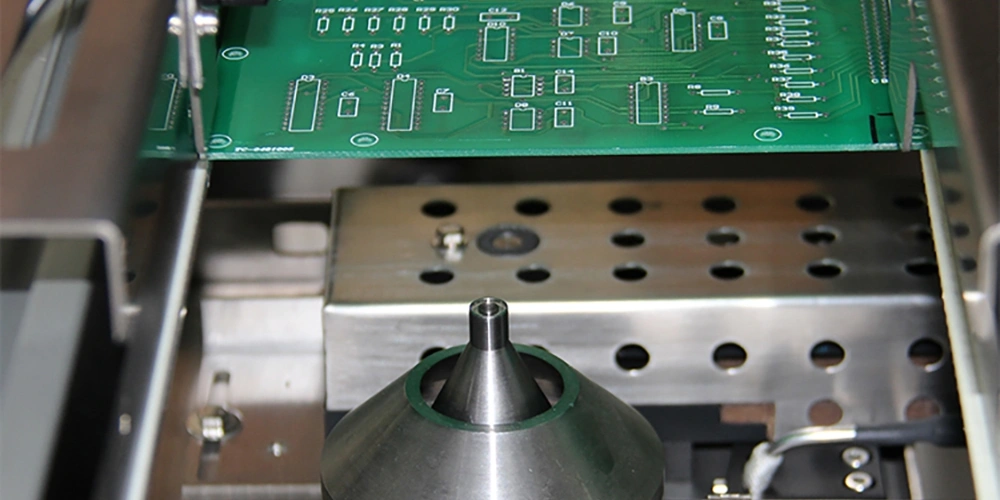
Selective soldering is a precise and programmable soldering process.
It uses an XYZ motion platform with a miniature solder nozzle or solder drag nozzle. The system applies solder only to specific THT pins that require soldering.
Unlike wave soldering, it does not immerse the entire PCB into solder. Instead, it creates solder joints one by one.
Why Does This Choice Matter?
There are three major reasons.
1. Thermal Shock Management
Wave soldering exposes the entire PCB to molten solder temperatures of approximately 230°C–260°C.
All components and PCB materials experience thermal expansion at the same time.
Selective soldering only heats specific target areas, greatly reducing the risk of:
- PCB warping
- Thermal damage
- Material stress
This is especially important for thin boards and high-density PCB designs.
2. Solder Masking and Fixture Requirements
In wave soldering, SMT components usually require protective fixtures or masking materials such as blue adhesive to prevent solder contact.
Selective soldering avoids this issue through software-controlled solder paths.
For high-density boards with fine spacing, removing fixture interference can become a major advantage.
3. Heavy Copper PCB Solder Joint Formation
For heavy copper PCBs with copper thicknesses up to 210 μm, insufficient preheating during wave soldering can cause excessive heat absorption through copper areas.
This may result in:
- Cold solder joints
- Poor solder penetration
Selective soldering can provide longer local heating and precise thermal control, improving solder filling performance in thick copper areas.
Materials and Process Factors in Soldering
Understanding how materials interact with both soldering methods helps prevent defects during PCB design.
Flux Chemistry and Application Strategy
Approximately 80% of soldering quality depends on flux performance.
In rapid PCB prototyping, flux selection must match the process requirements.
Wave Soldering Flux
Wave soldering usually uses:
- Rosin-based flux
- Low-solid-content no-clean flux
The flux is sprayed across the entire PCB surface.
Important factors include:
- Flux spreading ability
- Activation temperature range
The flux must activate properly during the preheat zone, usually around 100°C–130°C, and reduce surface tension when the PCB contacts the solder wave.
Selective Soldering Flux
Selective soldering uses point-sprayed flux.
The flux is only applied to the soldering pads that need processing.
This requires accurate rheological properties to prevent flux spreading into:
- High-frequency PCB microstrip areas
- Blind and buried via regions
This helps avoid unwanted changes in dielectric performance.
Pad Design and Through-Hole Solder Fill Requirements
PCB design determines whether soldering can be manufactured successfully.
According to IPC-A-610 Class 3, through-hole solder fill should exceed 75%.
Achieving this requirement depends on the soldering process.
Wave Soldering Through-Hole Filling
Wave soldering relies on the vertical pressure created by the solder wave.
When designing boards with large copper areas, such as aluminum-based PCBs, engineers must consider the fast heat dissipation caused by high thermal conductivity.
Solutions may include:
- Additional fixture-based thermal compensation
- Optimized solder contact time
Selective Soldering Through-Hole Filling
Selective soldering relies on:
- Nozzle movement
- Drag soldering
- Surface tension
For multilayer boards with buried copper planes, the small solder nozzle can provide controlled local heat for high aspect ratio holes and improve solder climbing performance.
Process Parameter Comparison
| Process Factor | Wave Soldering | Selective Soldering |
|---|---|---|
| Heat Source | Continuous molten solder wave | Precision mini solder nozzle / drag nozzle |
| PCB Contact Area | Entire bottom side contacts solder | Individual solder joints processed separately |
| Typical Preheat Temperature | 100°C–130°C (whole board) | 160°C–200°C (local bottom infrared heating) |
| Solder Contact Time | 2–5 seconds continuous | 1–3 seconds per solder joint, programmable |
| Flux Application | Full-board spraying | XY point spraying |
| Nitrogen Protection | Full tunnel nitrogen protection (optional) | Local nozzle nitrogen protection (standard) |
| Fixture Requirement | Required for SMT protection and solder mask areas | Usually unnecessary, controlled by programming |
| Minimum Spacing Requirement | >1.27 mm to reduce bridging | Down to 0.5 mm with precision nozzles |
| Suitable Board Thickness | 0.8–3.0 mm | 0.2–6.0 mm |
Soldering Process Flow and Quality Control
Understanding the complete process helps explain how automated production lines control quality.
Wave Soldering Process Steps
-
Through-Hole Component Insertion and Inspection
All THT components are inserted according to design requirements.
Automated equipment ensures accurate component positioning.
-
Fixture Loading
The PCB assembly is placed into a wave soldering carrier.
Precision fixtures are manufactured using:
- Mechanical machining
- Laser cutting
They protect sensitive SMT areas during soldering.
-
Flux Spraying
The PCB passes through the flux station.
Flux activates the solder pads and component leads.
-
Full Board Preheating
The PCB is gradually heated to:
- Remove solvents
- Activate flux
- Reduce thermal shock
For Metal Core PCBs, longer preheating time may be required.
-
Wave Contact
The PCB contacts the solder wave at a 3°–7° angle.
Surface tension removes excess solder and creates stable solder joints.
-
Cooling and Unloading
The PCB passes through the cooling zone and is removed from the carrier.
Selective Soldering Process Steps
-
Precision Flux Spraying
The programmable X/Y axis moves quickly between solder points and applies accurate amounts of flux.
-
Bottom Infrared Preheating
Focused infrared heating raises the temperature of the target solder area.
This prevents excessive heating of the entire PCB.
-
Dynamic Nozzle Soldering
The miniature solder nozzle follows a programmed path.
It can:
- Solder individual pins
- Drag solder multiple pins in a row
The process can be monitored through 3D AOI inspection.
-
Complete All Programmed Locations
The system automatically processes every required solder point.
Engineering Tip for Rapid PCB Prototyping
When activating selective soldering for rapid PCB assembly, always provide accurate nozzle selection instructions.
For THT pins below 0.5 mm pitch on rigid-flex PCBs, excessive solder can create hard stress points in the flexible area and cause future bending failures.
Key Decision Comparison
Choosing the wrong process during rapid prototyping can create unnecessary cost and reliability problems.
| Decision Factor | Wave Soldering Advantage | Selective Soldering Advantage | Selection Rule |
|---|---|---|---|
| Production Volume | Large volume, high UPPH | Small batch, prototypes, mixed production | Below 100 boards, selective soldering often avoids fixture costs |
| Component Density | Low density, component height <15 mm | Very high density with nearby SMT parts | If SMT components are within 2 mm of THT pins, choose selective soldering |
| Heat Sensitive Components | Higher process risk | Lower local thermal stress | Required for plastic connectors, capacitors, aluminum PCBs |
| Solder Quality | Depends on wave stability and conveyor speed | Depends on nozzle size and drag speed | Better for thick copper PCBs requiring controlled solder filling |
| Board Thickness | Best ≤3.0 mm | Up to 6.0 mm | Very thick boards require selective soldering |
| Process Cost | Fixture cost high but spreads over large volume | Programming cost only, no fixture cost | Better for low-volume prototypes |
| Oxidation Protection | Batch processing with tunnel nitrogen | Local nitrogen protection | Better surface protection, less impact on OSP |
How to Choose the Best Process
The decision should begin during the PCB design stage, not after production starts.
Evaluate Thermal Feasibility
Are you designing an 8 oz heavy copper PCB with fine-pitch components?
The large thermal mass of copper can absorb heat quickly during wave soldering, causing cold joints.
Selective soldering solves this by keeping the soldering heat directly at the joint location.
This is especially important for aluminum PCB and copper PCB applications.
Remove Spacing Conflicts
During DFM review, if a 0402 MLCC is within 0.8 mm of a THT pin on the bottom side, wave soldering is usually not suitable.
This is where selective soldering becomes the preferred solution.
The solder nozzle can avoid surrounding components without using masking tape.
Consider Fixture Economics
If your rapid PCB prototype requires only five boards, wave soldering fixtures can significantly increase the cost per board.
Selective soldering can directly generate solder paths from CAD data without waiting for fixture manufacturing.
This makes it ideal for 24-hour rapid PCBA assembly.
Control Soldering Sequence and Thermal Profile
For multilayer, blind/buried via, or high-frequency PCBs using selective soldering:
- Confirm peak temperature stays below the material Tg
- Plan soldering order carefully
- Start from the center and move outward
This prevents accumulated heat from causing solder mask discoloration or PCB damage.
Conclusion
Understanding the difference between wave soldering and selective soldering is not simply about choosing a machine.
It is about making PCB designs manufacturable.
The choice directly determines whether a mixed technology PCB achieves first-pass success or enters a cycle of repeated repair.
When your design requires high reliability, thermal control, and prototype cost efficiency, choosing a PCB manufacturing partner with both technologies is essential.
GREATPCB provides automated SMT production lines, 3D AOI inspection, and advanced selective soldering capabilities to connect your design requirements with real manufacturing processes.
From rapid PCB prototyping to advanced process review, our engineering team understands how to match the correct soldering profile for:
- Metal Core PCBs
- Heavy copper power boards
- High-density mixed technology assemblies
Frequently Asked Questions
Even a small number of bottom-side SMT components can be damaged by wave soldering.
Without proper fixtures, solder wave force may cause:
- Component movement
- Tombstoning
- Component detachment
Fixtures and adhesive processes add additional cost and process variables.
Selective soldering avoids these problems.
No, when properly controlled.
Selective soldering provides precise heat at individual solder points and usually uses closed-loop temperature monitoring.
As long as the local temperature stays below the material Tg, delamination can be avoided.
The key is choosing a manufacturer with accurate thermal process control.
This is highly risky.
Even if soldering occurs only on the rigid section, heat can transfer through copper into the flexible section.
This may cause:
- Adhesive failure
- Delamination
- Bubbling
- Flex layer wrinkles
Selective soldering is the safer industrial solution.
Technically yes, but only if the design already follows wave soldering DFM rules.
You need to reserve:
- Fixture space
- Component clearance areas
- Wave soldering process requirements
Otherwise, mass production conversion may require major PCB redesign.
The best approach is to discuss your final production process with the manufacturer during the initial rapid PCB prototyping stage.
Table of Contents
Tags
Related Posts
PCBA Prototype
August 7, 2026