How does the PCB assembly process work out?

How does the PCB assembly process work out?
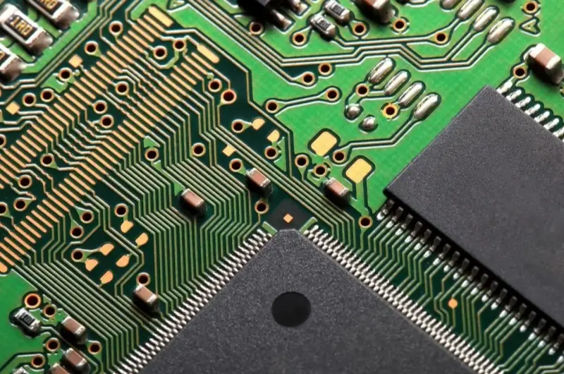
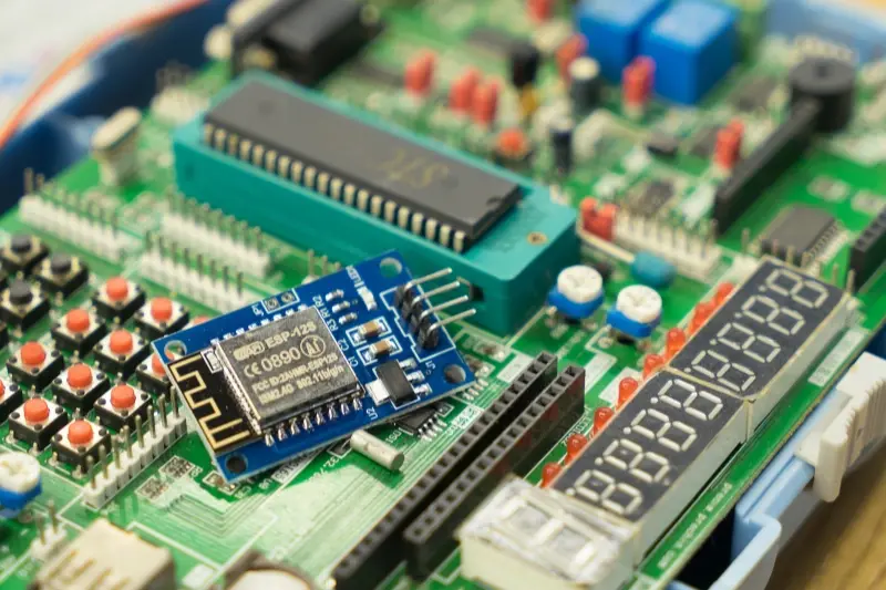
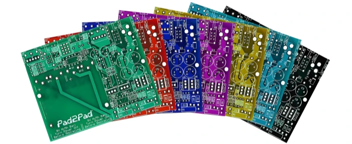
As we all know, Circuit board assembly is an important part of electronic PCB manufacturing, whether it is smartphones, computers, or medical devices, it is necessary to understand the relevant knowledge of printed circuit board assembly. Circuit board assembly is the process of installing and welding electronic components onto a printed circuit board. The PCBA manufacturer can use a variety of assembly techniques, including surface mounting technology (SMT), through-hole technology (THT), or a combination of both. After assembly, the PCB is tested to function properly before it can be integrated into the electronic device.
Understand the structure of PCB:
Circuit boards usually consist of several layers, each of which plays a crucial role in the function of the final product. The main layers include:
Substrates:
It is usually the bottom layer of the PCB board, usually made of epoxy resin (FR-4) reinforced glass fiber. It provides both the mechanical support and the insulation.
conducting layer:
These layers consisted of a thin copper foil laminated on the substrate. Conductive traces are etched on these foils to create the circuit path of the connecting elements.
Welding layer:
Composed of a thin copper foil laminated on the substrate. Conductive traces are etched on these foils to create the circuit path of the connecting elements.
Silk printing layer:
This layer contains markers such as component identifiers, logos, and other identification information. It can help technicians in assembly and troubleshooting.
The PCB manufacturing and assembly process
Manufacturability Design (DFM) inspection
Check the design specifications of the PCB and analyze any missing, redundancy, or potentially problematic features.
Inspection of electronic components
Our team of engineers will check whether the packaging, value, quantity, packaging, part number and other components of components match the BOM and PCB board.
Tin paste printing
The pad press applies the pad to a template and scraper.
Component placement
Place the components in a pre-planned area of the circuit board.
reflow soldering
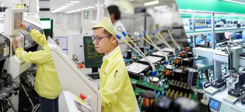
Attach the circuit board components, the components with the welding paste, and its components can be transported through the industrial grade reflux welding furnace. The heater in the oven melts the solder in the welding paste.
Product inspection
This stage helps to identify poor connection quality, misplaced components, and short circuits due to the continuous movement of the circuit board during the reflux process. PCB manufacturers use multiple inspection steps, such as visual inspection, automatic optical inspection, and X-ray inspection to check the functionality of circuit boards, identify low-quality solders, and identify any potential hidden problems.
Type of the PCB assembly process:
- SMT:
Surface mounting technology (SMT) is a method of mounting components to a circuit board.
- Through-hole assembly:
Through-hole assembly involves the insertion of element leads into pre-drilling before welding manually or by crest welding.
- Mixed assembly:
Through-hole technology (THT) and SMT are used simultaneously on the same plate, called hybrid assembly. It involves the use of surface mounting to weld components to the circuit board, and some special components cannot be fit through the SMT, requiring THT assembly on a hybrid PCB.
- Ball-grid array (BGA) assembly:
Ball grid array (BGA), also known as a chip carrier, is used to package integrated circuits (IC). They provide a means for the permanent installation of the microprocessors. Unlike traditional two-line or flat designs, the BGA can accommodate more connector pins.

Conclusion
Circuit board assembly is a complex but essential process in electronic fabrication. Understanding the layers, components, and manufacturing techniques involved provides an insight into the way electronic devices are manufactured. With companies like Great PCB offering reliable PCB manufacturing and assembly services, customers can confidently put their ideas into practice.
Table of Contents
Tags
Related Posts
PCBA Prototype
January 25, 2026
PCBA Prototype
December 8, 2025
PCBA Prototype
April 6, 2025


