PCB Design for Manufacturability (DFM)

Each PCB design should aim to minimize total costs and the potential for DFM issues (mostly a requirement from management, but whether engineers follow through varies by individual). Generally, this is accomplished through optimized PCB design techniques for conducting DFM checks.
DFM (Design for Manufacturing) is the process of arranging PCB layouts to address potential DFM issues that may arise during PCB assembly and manufacturing.
The key aspects include:
- What is manufacturability or DFM design in a PCB?
- Production-oriented PCB design (DFM)
- Common DFM errors in PCB manufacturing and preventive measures
1. What is manufacturability or DFM design in a PCB?
Simply put, DFM in PCBs is a set of design guidelines that ensure the manufacturability of electronic products, meaning that no issues arise during production.
Consider the consequences of encountering problems during the final manufacturing and assembly processes; you will “enjoy” dual scrutiny from both management and fellow engineers.
Of course, some manufacturers occasionally request unreasonable changes, where the design, its performance, or electrical requirements do not align.
1.1 DFM Analysis in PCBs
DFM analysis can identify manufacturing issues that may arise during assembly and manufacturing, primarily concerning PCB layout.
DFM issues are related to PCB geometry and, in most cases, cannot be detected during DFM checks.
1.2 Factors Influencing Design for Manufacturability
If the PCB performs well and the engineers are satisfied, why conduct a DFM manufacturability analysis? Is it due to a lack of technical proficiency from the engineers? Is it not trustworthy? (No offense intended toward engineers). There are various possibilities: the final PCB cost, design layout, and the likelihood of design failure.
- Theoretically, a PCB design submitted without DFM checks is cheaper than one with DFM checks; it is better to pay a little extra so the manufacturer can verify the design’s manufacturability.
- To maintain a PCB layout that has DFM issues, engineers edit the data to meet circuit design requirements, which is one of the main reasons signal integrity issues and EMI/EMC problems arise.
- Efficiently assembled and tested PCBs can still fail, primarily because the design data still includes DFM errors resolved in prototypes but not implemented during production.
2. Production-Oriented PCB Design (DFM)
DFM manufacturability analysis aims to solve problems before they arise.
DFM manufacturability analysis allows manufacturers to review the circuit board design from various aspects to effectively modify its materials, dimensions, and performance, enabling immediate detection of design issues and timely correction before production.
A step-by-step design approach for manufacturability analysis includes the following attributes:
- Identifying design violations that will impact PCB manufacturing.
- Determining precise manufacturing processes based on PCB geometry and material requirements.
- Inspecting PCB designs to ensure specifications align with finished products.
- Selecting materials based on board size (considering characteristics, physical strength, and texture).
- Ensuring designs adhere to specified rules to meet quality standards and reliability.
3. Common DFM Errors in PCB Manufacturing and Preventive Measures
Copper Strips Prevention
Thin strips are wedge-shaped sections of dry film resist that expose copper and create short circuits. Strips can be conductive (copper) or non-conductive (solder mask).
Causes of Copper Strip Formation
Two main reasons lead to strip formation:
- Long, thin features of copper or solder mask are etched away; during manufacturing, separated long copper strips can lead to short circuits.
- Cutting too close or too deep to part of the PCB design can adversely affect its functionality.
Solutions for Copper Strips
Implement a minimum photoresist width to avoid this defect, applying the same net spacing (less than 3 mils) or removable or filled gaps. Proper DFM analysis is essential to identify areas where strips may form and resolve the issues (if any).
Selection of PCB Electronic Components
Component selection should be based on availability, lead time considerations, and monitoring of obsolete or discontinued parts to ensure components can be sourced before manufacturing begins.
- Identify component and package sizes through thorough BOM research; if there is enough space, opt for larger components for resistors and capacitors. For instance, use 0603 or 0805 sized capacitors/resistors instead of 0402/0201.
- Choose components less affected by voltage, current, and frequency.
- If possible, select smaller packages; overuse of small component packages complicates PCB assembly, making cleaning and rework more difficult.
Test Points
DFM manufacturability analysis includes test points for all critical signals to check electrical connections after the circuit board is built. If excluded, it becomes challenging to verify the final product. Here are some tips to avoid potential manufacturing issues:
- Place all test points on the same side of the circuit board for easier testing.
- Maintain a minimum distance of 0.100 inches between test points to enhance testing efficiency.
- Specify higher component mounting areas.
- Distribute all test points evenly for easy access with multiple probes.
- Keep manufacturing tolerances in mind when designing layouts.
Through Holes and Drill Copper
(1) Drill Holes and Hole Diameter
Drill copper refers to the distance from the edge of the hole to the nearest copper feature. However, PCB layout engineers consider the distance from the finished hole size (FHS) to the nearest copper feature.PCB layout engineers should always consider drill hole diameter (FHS + drill tolerance) to determine the proper distance. Drill hole diameter can be calculated as follows:
Finished Hole Size+Tolerance=Drill Diameter\text{Finished Hole Size} + \text{Tolerance} = \text{Drill Diameter}Finished Hole Size+Tolerance=Drill DiameterGenerally, the distance should be 5-8 mils, depending on the number of layers.

(2) Drilling to Copper Gaps
In ringed holes, tangential or breaks may occur when the drill fails to reach the desired position and deviates along the same axis. This can cause edge interconnections and affect reliability.
(3) Annular Ring
Here are some tips to avoid DFM manufacturability issues during drilling:- Ensure good conductivity and ease of drilling holes in pads by incorporating a wider annular ring area in your design by adjusting pad sizes.
- Verify that plated drill holes have copper pads on all layers.
- A minimum of 8 mils between drill and copper is recommended.
- Maintain a minimum aspect ratio to prevent misalignment of the drill.
- Define hole types (PTH/NPTH) and count/size of holes.
- Ensure copper functionality and holes fit the PCB profile.
- Design an annular ring size equal to or larger than the minimum circle size (4 mil) that the vendor/manufacturer can produce.
- Add teardrops to prevent ring breakage in complex designs and smaller annular rings.
Matching Drill Counts to Drill Charts
It is crucial to match drill counts with the drill charts.
The fab drawing contains the drill hole chart; sometimes, the drilling chart does not match the actual drill count, in which case you will need to modify or regenerate the drilling chart.
As a simple design point, minimize the number of different drill sizes used in the PCB layout. It is best to select one or two through-hole sizes to handle most signal layer transitions and potentially choose a few others for mounting holes or non-plated through holes.
Gaps
In PCB DFM manufacturability production, three types of gaps must be observed.
(1) Edge Gaps:
Some PCB layout engineers forget to provide sufficient gaps between copper and the PCB edge. If current is applied to adjacent layers, the proximity of copper to the edge can create short circuits between adjacent layers, resulting from exposed copper at the PCB periphery.Increasing the gap in your design can resolve edge gaps. Check the following approximate values:
- Outer layers: 0.010”
- Inner layers: 0.015”
(2) Trace Spacing:
Trace spacing is the minimum distance between two conductors, which depends on materials, copper weight, temperature variations, and applied voltage, as well as the manufacturer’s capabilities.(3) Solder Mask Gap:
Maintain solder mask gaps greater than pads, except for solder mask-defined pads. The best way to prevent solder bridges is to extend the mask openings to copper pads or provide barrel-shaped relief (solder mask gap = drill size + 3 mil).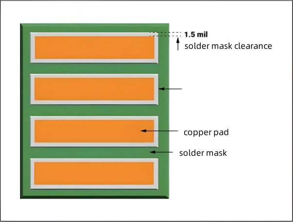
Missing Solder Mask
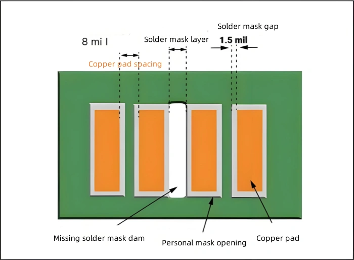
Occasionally, the solder mask may be partially or entirely absent between pads, exposing excess copper and resulting in solder bridges and short circuits that affect PCB performance.
This occurs when the solder mask is not defined, or a larger PCB setting is applied to a smaller PCB, leading to larger pad holes.
Recommended solder mask design tips include:
- The relative size of the solder mask should be larger than the feature size by 4 mil.
- Maintain solder mask width/bridging at least 4 mil.
- Keep a 2 mil spacing between copper feature edges and solder paste edges.
Acid Traps
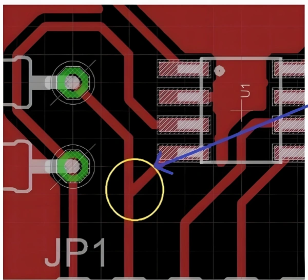
Another DFM error to watch for is acid traps. Designs containing sharp angles can attract acid concentration to that area, potentially leading to over-etched traces and open circuits.
Avoid routing traces to pads at sharp angles; position traces at 45° or 90° relative to pads, and verify that no trace angles create acid traps after etching.
Silkscreen Inspection
Silkscreen inspection involves various attributes that can impact DFM manufacturability and prevent potential errors. Here are some suggestions:
(1) Orientation
Silkscreen may be located on pads, which should be checked by running a DRC (Design Rule Check).Silkscreen can also overlap with vias, although this is acceptable if the vias are tented. This may occur when rotating text or adjusting component reference designator markings.
Trim reference designator markings that cross over pads and vias to prevent overlapping.
Ensure your silkscreen orientation is consistent.
(2) Line Width and Text Height
It is generally recommended to use a minimum line width of 4 mils and a text height of 25 mils for readability.Always use standard colors and larger shapes for good performance. Typically, sizes should be 35 mils (text height) and 5 mils (line width).
If the board is not dense and there is enough space to place larger text, the following sizes are recommended:
Line Width and Text Height Table Line Width (mil) 5 Text Height (mil) 35 If the above specifications are not suitable for medium-density boards, the following sizes are recommended:
Line Width and Text Height Table Line Width (mil) 6 Text Height (mil) 40 When the above sizes are not feasible, for medium-density boards, the following sizes are recommended:
Line Width and Text Height Table Line Width (mil) 7 Text Height (mil) 45 (3) Silkscreen Methods
The specific methods used can affect many design parameters, such as dimensions, spacing, and elements like pads, vias, and traces.Specify the silkscreen method based on manual silkscreen, liquid photo imaging, and direct legend printing.
Marking priority: Prioritize silkscreen markings based on categories: regulatory requirements, manufacturer identification, assembly aids, and test aids.
DFM for PCB Layout
1. SMT Devices
The spacing of component layouts must meet assembly requirements. Generally, surface-mounted devices (SMDs) should have a spacing greater than 20 mils, ICs greater than 80 mils, and BGAs greater than 200 mils. Adequate spacing between components during layout enhances the yield of the manufacturing process.
The spacing between SMD pad pins should generally be greater than 6 mils. The manufacturing capability of solder mask bridges is 4 mils. If the SMD pad spacing is less than 6 mils and the solder mask opening spacing is less than 4 mils, the solder mask bridge cannot be retained, resulting in excessive solder during assembly (especially between pins), which may lead to short circuits.
2. DIP Devices
For devices undergoing wave soldering, pin spacing, device orientation, and spacing must all consider the requirements of the wave soldering process. Insufficient pin spacing can lead to solder bridging, which in turn causes short circuits.
Many designers try to minimize the use of through-hole components (THT) or place them on the same side of the board. However, through-hole components are often unavoidable. In a combined scenario, if through-hole components are placed on the top layer and surface-mounted components on the bottom layer, this may affect single-sided wave soldering. In such cases, more expensive soldering techniques, like selective soldering, must be used.
3. Distance from Components to Board Edge
For machine soldering, electronic components are generally required to be 7 mm away from the board edge (requirements may vary by soldering manufacturer). However, during PCB fabrication, process edges can be added to allow electronic components to be placed at the board edge, as long as wiring is facilitated.
However, components near the board edge may encounter the machine’s guide rails during soldering, potentially damaging the components. Pads for components at the board edge may be trimmed during the manufacturing process; if the pads are small, this may impact soldering quality.
4. Distance between Tall and Short Components
There is a wide variety of electronic components, each with different shapes and lead configurations, leading to variations in assembly methods. A good layout not only stabilizes machine performance, reduces vibration, and minimizes damage but also achieves a neat and aesthetic appearance within the device.
A certain distance must be maintained around tall components for shorter components. If the distance between components is smaller than the height of the components, uneven hot airflow may occur, leading to soldering defects or the risk of non-repairable solder joints.

5. Spacing Between Components
In general SMT assembly, it is essential to consider the installation accuracy of the machine, as well as maintenance and visual inspection. Adjacent components should not be too close together, leaving a safe distance.
The spacing between chip components, SOTs, and SOICs should be 1.25 mm. The spacing between PLCCs and chip components, SOICs, and QFPs should be 2.5 mm, while the spacing between PLCCs should be 4 mm. When designing PLCC sockets, care should be taken to accommodate the dimensions of the PLCC socket (the pins of the PLCC are located on the inner side of the socket).
DFM for PCB Routing
1. Line Width / Spacing
For designers, it is essential not only to consider the precision and perfection of the design but also the constraints imposed by manufacturing processes. PCB manufacturers cannot reinvent a production line for the sake of producing an exceptional product.
Typically, the standard control for line width and spacing is 4/4 mils, with vias selected at 8 mils (0.2 mm), which is achievable by over 80% of PCB manufacturers, resulting in the lowest production costs. The minimum control for line width and spacing is 3/3 mils, with vias selected at 6 mils (0.15 mm), achievable by over 70% of PCB manufacturers, albeit at a slightly higher cost than the first scenario.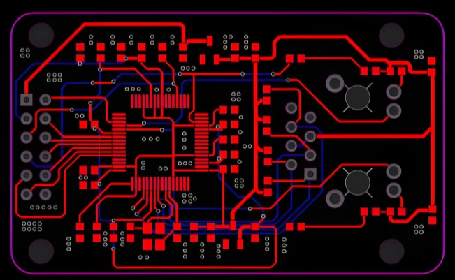
2. Sharp Corners / Right Angles
Sharp corners in routing are generally prohibited, while right angles should be avoided as much as possible in PCB routing; this has almost become a standard for measuring the quality of routing. Right-angle routing can adversely affect signal integrity, generating additional parasitic capacitance and inductance.
3. Copper Strips / Islands
If there are sufficiently large copper islands, they can act as antennas, potentially causing noise and other interference within the circuit board (as the copper is not grounded, making it a signal collector).
Copper strips and islands floating on multiple plane layers can lead to severe issues in the acid tank. It is well known that small copper spots can detach from the PCB panel and migrate to other etched areas on the panel, resulting in short circuits.
4. Hole Rings
Hole rings refer to the copper surrounding a drilled hole. Due to tolerances in the manufacturing process, the remaining copper ring around a drilled hole may not perfectly align with the pad center, potentially leading to the breakage of the ring.
Via hole rings should be greater than 3.5 mils on one side, while through-hole rings should be greater than 6 mils. If the ring is too small during manufacturing, tolerances in drilling and alignment can cause the ring to break, resulting in open circuits.

5. Routing Teardrops
Adding teardrops to PCB routing can enhance the stability and reliability of connections on the board, ensuring a more stable system. Therefore, incorporating teardrops in the circuit board design is necessary.

Teardrops can prevent the points of contact between wires and pads or wires and vias from breaking under significant external force. They also protect pads during soldering, preventing detachment from repeated soldering and reducing the risk of uneven etching and cracks from via misalignment during production.
Related Posts
PCBA Prototype
January 25, 2026
PCBA Prototype
December 8, 2025


