PCB Grounding Design and Layout Best Practices
1. Ground Wire All parts that are connected to ground are linked together through one common trace. This is common in old PCB designs and in simple PCB designs. 2. [...]
1. Ground Wire All parts that are connected to ground are linked together through one common trace. This is common in old PCB designs and in simple PCB designs. 2. [...]
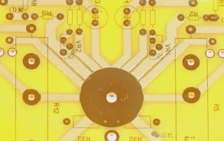
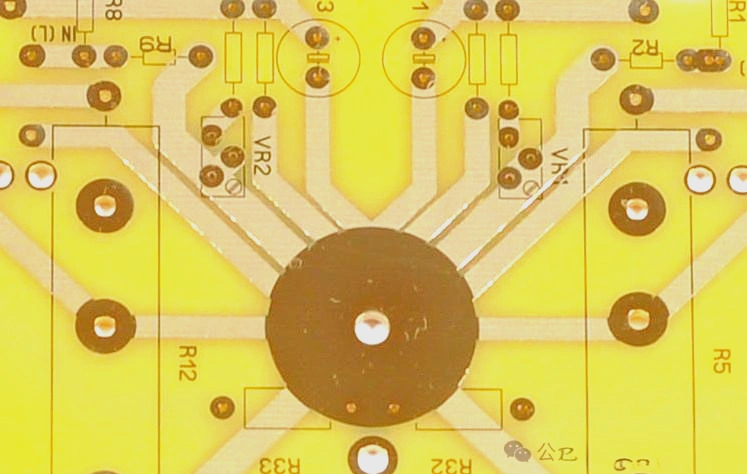
PCB grounding is a topic that PCB layout engineers always care about. For example, how should an effective grounding system be planned on a board? Should all the analog ground, [...]
Introduction In the contemporary era of rapid technological advancement, microwave PCB design has emerged as a linchpin in modern electronic devices, wielding profound significance across diverse high - tech arenas. [...]
In the field of electronic circuits, the impedance matching of SPI signal lines is of utmost importance, especially in high - speed application scenarios. SPI (Serial Peripheral Interface), as a [...]
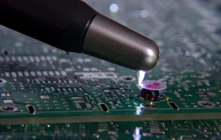
Today, the reduction in the size of basic circuit boards will allow designers to shrink their PCB dimensions by half, or even down to a quarter of the original size. [...]
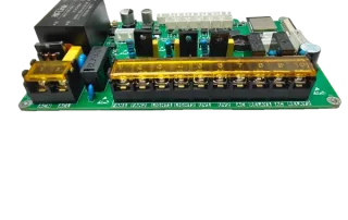
1. What is High-Power PCB? High-power PCB is a printed circuit board made of heavy copper. Compared to other circuit boards, high-power PCBs can handle higher current rates, withstand high [...]
PCB design requires meticulous thought; the more thoughtful and experienced a designer is, the better the resulting board. 1. Preparation Stage: This involves preparing the component library and schematic. To [...]
Each PCB design should aim to minimize total costs and the potential for DFM issues (mostly a requirement from management, but whether engineers follow through varies by individual). Generally, this [...]


