Mastering PCB Design: A Step-by-Step Guide

PCB design requires meticulous thought; the more thoughtful and experienced a designer is, the better the resulting board.
1. Preparation Stage:
This involves preparing the component library and schematic. To create a good board, not only is it essential to design the schematic properly, but drawing the board is also a critical part. Before starting PCB design, ensure that the component library for the schematic (SCH) and the PCB is ready. While you can use the libraries provided by the design software, they often lack suitable options, so it’s best to create your own based on the standard dimensions of the selected components. Ideally, start with the PCB component library, followed by the SCH library. The PCB library has stricter requirements as it directly affects the board’s installation; the SCH library is more lenient, focusing on defining pin properties and their correspondence with PCB components (pay attention to hidden pins in the standard library). Afterward, design the schematic, and once completed, you can start PCB design.
2. PCB Structure Design:
Based on the determined board dimensions and mechanical positioning, draw the PCB layout in the design environment, placing required connectors, buttons/switches, screw holes, assembly holes, etc. Consider and define wiring and non-wiring areas (e.g., how large an area around screw holes is designated as a non-wiring area).
3. PCB Layout:
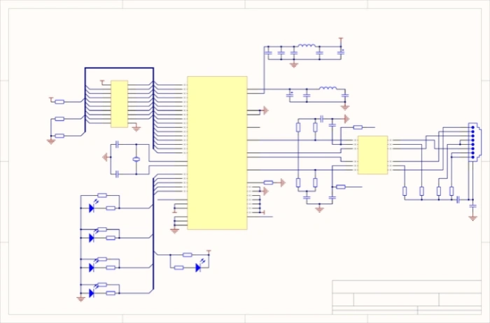
Layout simply means placing components on the board. If the previous preparation is done correctly, you can generate a netlist from the schematic (Design -> Create Netlist) and then import it into the PCB layout (Design -> Load Nets). You’ll see all components stacked with fly lines indicating connections. Now, you can begin the component layout based on the following principles:
- Reasonably partition based on electrical performance, generally into: digital circuit area (susceptible to interference and generating interference), analog circuit area (sensitive to interference), and power drive area (interference source).
- Components completing the same function should be placed as close as possible, adjusting to ensure the simplest connections; also, adjust the relative positions of functional blocks to simplify interconnections.
- For heavier components, consider installation position and strength; heat-generating elements should be placed separately from temperature-sensitive components, and thermal convection measures should be considered if necessary.
- I/O driver components should be placed near the edge of the board and close to connectors.
- Clock generators (e.g., crystal oscillators) should be placed as close as possible to the devices that use the clock.
- A decoupling capacitor should be placed between the power input and ground pins of each integrated circuit (generally a high-frequency ceramic capacitor); for densely packed circuits, consider adding a tantalum capacitor around several integrated circuits.
- A discharge diode (e.g., 1N4148) should be added to the relay coil.
- The layout should be balanced and orderly, avoiding being top-heavy or too cluttered.
It is crucial to consider the actual size (area and height) of components and their relative positions to ensure the electrical performance and feasibility of production and installation. Additionally, under the premise that the above principles can be reflected, adjust component placement for neatness and aesthetics—similar components should be arranged uniformly and consistently, avoiding a “scattered” appearance. This step affects the overall image of the board and the ease of the subsequent wiring, so significant effort should be dedicated to it. During layout, for uncertain areas, preliminary wiring can be done for thorough consideration.
4. Wiring:
Wiring is the most critical step in the entire PCB design process, directly affecting the PCB’s performance. There are generally three levels of wiring: First is basic connectivity—if the wiring is not connected and there are numerous fly lines, the board is considered unqualified. Second is meeting electrical performance requirements, which is the standard for determining whether a PCB is qualified. After achieving connectivity, carefully adjust the wiring for optimal electrical performance. Finally, there’s aesthetics; if your wiring is connected but looks chaotic and colorful, regardless of good electrical performance, it may be perceived as poor quality, complicating testing and maintenance. Wiring should be neat and orderly, avoiding chaotic crossings. These considerations must be balanced with electrical performance and other specific requirements; otherwise, the design may lose focus.
When wiring:
- Typically, start with power and ground wiring to ensure electrical performance. If conditions allow, widen the power and ground wire widths, ideally making the ground wider than the power line, following the hierarchy: ground > power > signal. Signal line widths typically range from 0.2 to 0.3 mm, with a minimum width of 0.05 to 0.07 mm; power lines range from 1.2 to 2.5 mm. For digital PCBs, a wide ground wire can form a loop, creating a ground net (this is not suitable for analog circuits).
- Pre-wiring for stricter requirements (like high-frequency lines) should avoid adjacent parallel input and output edge lines to minimize reflection interference. Ground isolation may be necessary; wiring on adjacent layers should be perpendicular, as parallel wiring can cause parasitic coupling.
- Ensure the oscillator housing is grounded; keep clock lines short and avoid unnecessary extensions. The ground area beneath the clock oscillator circuit and special high-speed logic circuit sections should be increased, avoiding interference from other signal lines.
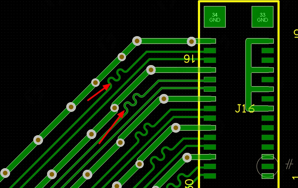
- Use 45-degree angles for wiring instead of 90 degrees to reduce high-frequency signal radiation (for high-demand lines, consider using double arcs).
- Signal lines should not form loops; if unavoidable, keep them as small as possible; minimize vias for signal lines.
- Critical lines should be kept short and thick, with protective grounding on both sides.
- Use a “ground-signal-ground” configuration when transmitting sensitive signals and noise via flat cables.
- Key signals should have test points reserved for production and maintenance.
- After schematic wiring is complete, optimize the wiring; upon initial network check and DRC check verification, fill unconnected areas with ground, using large copper layers for ground connections, connecting unused areas on the PCB as ground. Alternatively, consider multilayer boards, allocating one layer each for power and ground.
PCB Wiring Process Requirements
- Lines: Generally, signal lines should be 0.3 mm (12 mil), power lines 0.77 mm (30 mil) or 1.27 mm (50 mil); spacing between lines and between lines and pads should be ≥ 0.33 mm (13 mil). In high-density applications, consider using two lines between IC pins, with widths of 0.254 mm (10 mil) and a minimum spacing of 0.254 mm (10 mil). Under special circumstances, when component pins are close, consider reducing width and spacing appropriately.
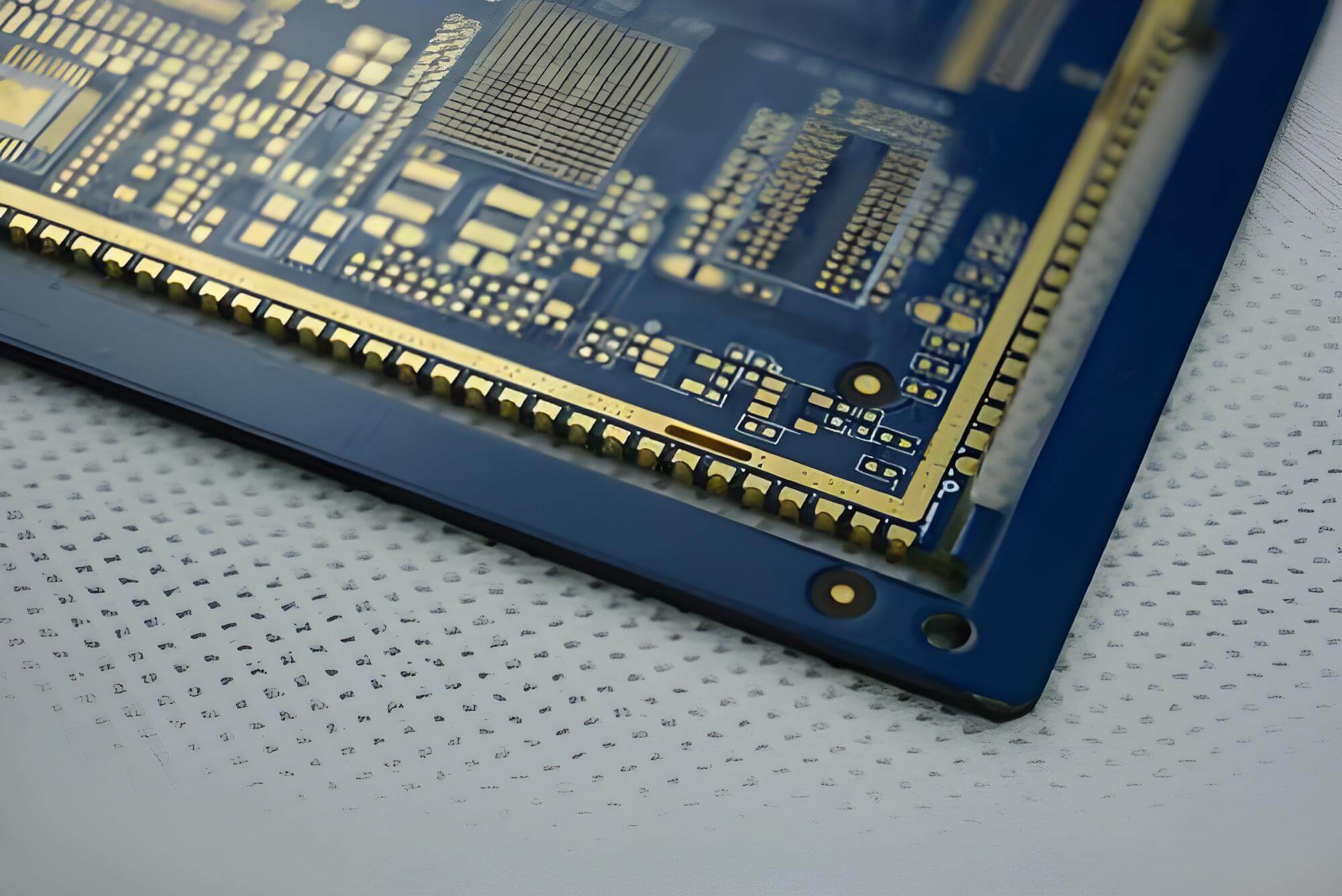
- Pads: Pads (PAD) and vias (VIA) must meet basic requirements: pad diameter should be ≥ 0.6 mm larger than the hole diameter; for example, use pad/hole sizes of 1.6 mm/0.8 mm (63 mil/32 mil) for general leaded resistors, capacitors, and ICs, and 1.8 mm/1.0 mm (71 mil/39 mil) for sockets, pins, and diodes like 1N4007. In practice, size pads according to actual component dimensions, and if possible, slightly increase pad sizes.
- Vias: Standard via size is 1.27 mm/0.7 mm (50 mil/28 mil). In high-density wiring scenarios, the via size can be reduced, but not excessively, possibly using 1.0 mm/0.6 mm (40 mil/24 mil).
- Spacing Requirements for Pads, Lines, and Vias:
- PAD and VIA: ≥ 0.3 mm (12 mil)
- PAD and PAD: ≥ 0.3 mm (12 mil)
- PAD and TRACK: ≥ 0.3 mm (12 mil)
- TRACK and TRACK: ≥ 0.3 mm (12 mil) In high-density situations:
- PAD and VIA: ≥ 0.254 mm (10 mil)
- PAD and PAD: ≥ 0.254 mm (10 mil)
- PAD and TRACK: ≥ 0.254 mm (10 mil)
- TRACK and TRACK: ≥ 0.254 mm (10 mil)
5. Wiring Optimization and Silkscreen:
“There is no best, only better!” Regardless of how thoughtfully you design, once finished, you’ll find many areas for modification. Generally, the time spent optimizing wiring is twice that spent on initial wiring. Once satisfied with the layout, copper can be poured (Place -> Polygon Plane). Copper is typically applied to ground (noting the separation of analog and digital grounds), and for multilayer boards, power may also require copper. Regarding silkscreen, ensure it doesn’t obstruct components or get covered by vias and pads. When designing, text on the bottom layer should be mirrored to avoid confusion.
6. Network, DRC Checks, and Structural Inspection:
First, ensure the circuit schematic design is correct. Then, perform a physical connection check (NETCHECK) between the generated PCB network file and the schematic network file, promptly making adjustments based on output results to guarantee correct wiring connections. Once network checks pass, conduct a DRC check and adjust the design based on output results to ensure PCB wiring meets electrical performance. Finally, further inspect and confirm the mechanical installation structure of the PCB.
7. Fabrication:
Before this, it’s best to have a review process.
PCB design requires extreme attention to detail, considering all factors and striving for perfection to ensure the creation of a good board.

Related Posts
PCBA Prototype
July 21, 2026
PCBA Prototype
July 17, 2026