PCB Design: Unveiling the Misconceptions of Right-Angle Routing

It is widely known that PCB routing should avoid right angles or acute angles. This rule is emphasized in textbooks and company technical specifications, and some even use it as a benchmark to judge someone’s experience level. However, the reasoning behind this rule can be somewhat puzzling.
Reasons Against Right Angles
There are three main reasons for avoiding right angles in PCB routing:
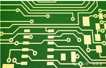
- Signal Integrity: At right-angle bends in PCB traces, the signal’s leading and trailing edges can affect each other, increasing distributed capacitance and delaying the signal’s rise and fall times. From an impedance perspective, the width of the trace increases at the right angle, causing impedance discontinuity, which results in signal reflection and impacts signal integrity.
- Electromagnetic Radiation: Sharp angles can lead to increased electromagnetic radiation or discharge.
- Manufacturing Issues: During the PCB copper etching process, corrosive liquid tends to accumulate at sharp angles, potentially causing excessive corrosion and resulting in broken traces.
Analysis of Reasons
- Impedance Changes and Parasitic Capacitance: The impedance change caused by right-angle routing can be calculated using empirical formulas. For example, a PCB trace with a characteristic impedance of 50Ω and a width of 4 mils will experience a distributed capacitance change of approximately 0.01 pF at a right angle.Thus, the capacitive effect of right-angle routing is minimal.

- Impedance changes at right angles are generally between 7% and 20%, with a maximum reflection coefficient of around 0.1. Therefore, the impedance change due to right or acute angles is relatively minor and has a negligible effect on signal integrity. For frequencies above 10 GHz, PCB traces should ideally use curved bends. In typical designs, the angle of bends, whether 40°, right angles, or any other angles, has minimal impact on signal quality.

- Electromagnetic Radiation and Discharge: Sharp angles could theoretically cause discharge if the voltage is high enough to break down air or the PCB’s insulating layers, but such high voltages are rare in typical circuits. The impact of sharp angles on EMI (electromagnetic interference) is also minimal, with no substantial evidence supporting significant emissions or receptions.

- Manufacturing Issues: Historically, PCB production used acidic etching solutions, which could lead to over-etching at sharp angles. However, since the 1990s, advancements in etching solutions and photoresists have largely resolved this issue.
Conclusion
Overall, the rule against using right angles in PCB routing does not seem to have strong justification. For circuits operating below 100 GHz, the impact of sharp or right-angle bends on signal integrity is negligible. Instead, factors like component placement, ground design, trace width, and vias have a more significant impact and should be considered more carefully.
Why Are We Still Taught to Use Rounded Angles?
According to the analysis above, right angles have no particular disadvantages but offer no specific advantages either. Using 135° obtuse angles is safer and may be influenced by historical and traditional reasons that have established industry habits and aesthetic preferences. Unless aiming for a unique design, right and acute angles are rarely used. This article does not advocate for right-angle routing but rather advises not to rush into criticizing PCB designs that include right or acute angles.


