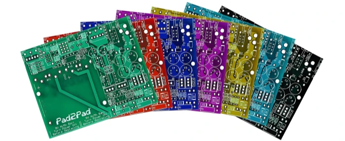
PCB Reverse Engineering Guide: Easily Replicate Designs

PCB reverse engineering refers to the process of obtaining a physical PCB and conducting research to analyze its characteristics and wiring layout. In earlier reverse engineering efforts, the primary focus was on deducing the schematic diagram by reverse-engineering PCB design files or sketching a PCB circuit diagram directly from the physical product. This allows for understanding the board’s circuitry and functionality. The schematic is also used to analyze the product’s features.
Purpose of Reverse Engineering:
Some companies may find an impressive product and purchase it to study how the PCB was designed and manufactured. After conducting reverse engineering, they can determine aspects like copper thickness, roughness, pad dimensions, trace widths, compensations, etc. By doing this, they gain critical insights into their competitor’s design, which can be replicated or improved upon. However, even after obtaining the standard parameters, manufacturing methods and control processes may still vary greatly across different companies. Customer blueprints and Gerber files generally specify the final product’s specifications, and manufacturers measure and test the boards according to their standards. GREATPCB, for instance, can restore these designs with high accuracy.
Reverse Engineering Process:
The reverse engineering process for PCBs and PCBA varies slightly but follows similar overall steps.
- Recording Key Information:
For a PCBA, components’ details such as model parameters and precise locations must be recorded. Before desoldering the components, they are scanned or photographed, ensuring all part information, especially diodes and transistors, is visible and unobstructed. - Component Removal:
The components are desoldered in a specific order (resistors, capacitors, then ICs), with care taken to record any missing or misplaced parts. The desoldered components are measured using tools like a bridge circuit after cooling to ensure accurate readings. - Surface Cleaning:
Remaining solder and debris are removed with cleaning agents, ensuring the PCB is in good condition for further steps. - Image Adjustment and Verification:
Scanned images of the PCB are enhanced and adjusted for contrast and clarity. The images are then converted to a format that design software can interpret for further analysis. - PCB File Creation:
Using design software such as Protel, top and bottom PCB layers are traced, and components are placed on the schematic to reconstruct the PCB layout. - Verification and Testing:
The printed PCB layout is compared to the original to check for consistency, followed by testing the circuit’s functionality.
Challenges of Reverse Engineering:
Reverse engineering is complex and highly dependent on the skill level of the technicians involved. Beyond mastery of basic techniques, patience, and meticulousness are critical in ensuring accuracy when analyzing and reconstructing the circuit.
Trade-Off Between Reverse Engineering and Original R&D:
For highly intricate boards, reverse engineering can be very difficult and costly, especially if the process fails, as it affects both the project timeline and budget. While original R&D can also be time-consuming and require hiring technical experts, one of the best approaches is to work with a one-stop manufacturer, like GREATPCB, to handle the entire process from product development to programming and assembly.
Table of Contents
Related Posts
PCBA Prototype
May 14, 2026


