2-layer high-density PCB prototyping
By PCBA PrototypePublished On: 2026-06-16Categories: Blog0 Comments on 2-layer high-density PCB prototyping
By PCBA PrototypePublished On: 2026-06-16Categories: Blog0 Comments on 2-layer high-density PCB prototyping

Some information about 2-layer high-density PCB prototyping:
| Type | PCB & PCB Assembly |
| Industry experience | 15+years |
| Place of Origin | Baoan,Shenzhen,China |
| Company Name | GREATPCB |
| Product Features | Vibration resistant,High precision,High temperature resistance,High Qulity,Environmentally Friendly,Smaller Size… |
| Certificate | IS014001,IS045001,ITAR REGISTERED,MIL-PRF-31032… |
| OEM/ODM | Support |
| Surface treatment | ENEPIG,ImAg,Electrolytic Hard Gold,HASL,ImSn,ENIG… |
| Application | Computers & Networks,Automotive Electronics,Consumer Electronics,Medical Equipment,Industrial Control,AI & Data Center…etc |
| Design Software | Mentor PADS,Altium Designer,Cadence Allegro,AutoCAD… |
| Payment | Google Play,Visa,T/T…etc |
| Nearby ports | Shenzhen… |
| Warranty | 1 year |
| One Stop Services | Sourcing Components ,Programming IC,Conformal Coating, Function and Aging Testing |
| Transportation | UPS,EMS,TNT,DHL…etc |
| Packing Size | 94 * 25 * 91 According to container size, standard export package |
| Terms of delivery | Western Union,Cash,L/C… |
| Operating Temperature | -40°C to 125°C |
| Solder mask Color | Green,Yellow,Red, or according to customer requirements |
| Material | FR4 /aluminum/ceramic CEM1 |
| After-sales Service | Online support |
| Trading Country | Mid east,Africa,Southeast asia,Europe,British,Australia,South Africa,Russia,Korea… |
| Selling Units | Single item |
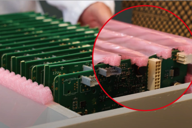
Some PCB & Switch Module & Elevator Relay
Our workshop for 2-layer high-density PCB prototyping

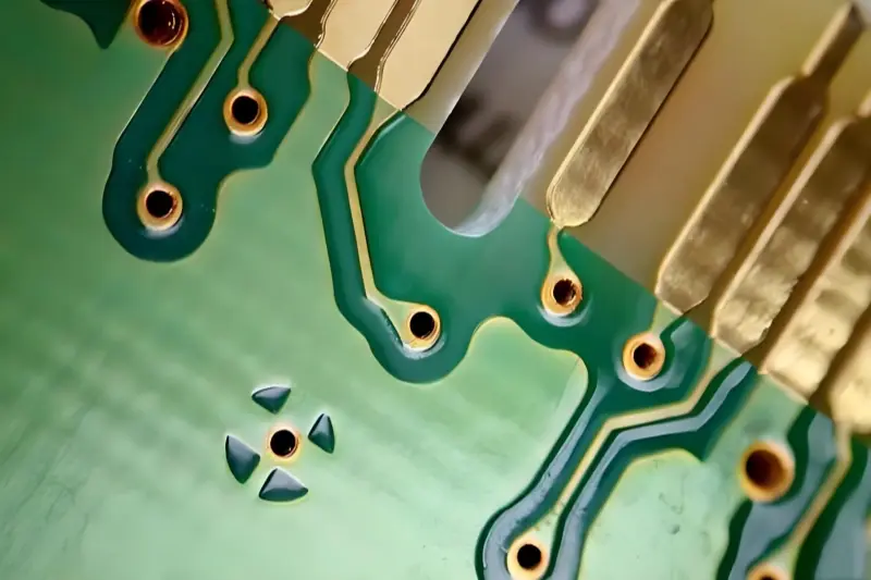
Advanced PCB manufacturing equipments

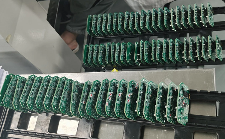
The test for 2-layer high-density PCB prototyping

Table of Contents

Tags
Related Posts
PCBA Prototype
July 17, 2026